English
Views: 0 Author: Site Editor Publish Time: 2026-04-22 Origin: Site


In the rapidly advancing field of power electronics, reflow soldering plays a critical role in assembling power control devices such as inverters, power supplies, and electric vehicle (EV) systems. These components are essential in managing energy conversion and distribution, often in high-power applications.
However, the challenges associated with reflow soldering for power electronics PCBA (Printed Circuit Board Assembly) are substantial due to the unique requirements of power components.
This article discusses the major reflow soldering challenges faced by power electronics, including thermal management, PCB warpage, soldering defects, and the optimization of temperature profiles.
Additionally, we will explore advanced techniques and the integration of automation and quality control to improve the reflow soldering process for power electronics.
Power electronics often involve high-power components like power semiconductors and large capacitors, which tend to have a high thermal mass. This means they take longer to heat up and cool down compared to smaller components. In reflow soldering, achieving uniform heating across the entire PCB is crucial. The presence of high thermal mass components can cause uneven heating, leading to localized temperature variations that can compromise solder joint integrity.
This is particularly problematic when dealing with delicate components that are sensitive to excessive heat, making uniform temperature control critical for high-quality soldering.
Another thermal challenge in power electronics PCBA reflow soldering is the risk of thermal shock. The high thermal gradients created during the heating and cooling phases of reflow soldering can cause components to expand and contract at different rates. This difference in expansion can lead to the cracking or fracture of components, especially in high-power modules that have complex designs.
Additionally, solder joints may fail if the temperature change is too rapid. Managing thermal profiles and reducing the likelihood of thermal shock is essential for ensuring long-term reliability and performance.

Power electronics PCBs often have heavy copper layers, large copper planes, and a variety of components with different sizes and weights. The difference in the coefficients of thermal expansion (CTE) between the PCB material (typically FR4) and the copper or other metal components can cause PCB warpage. Warping occurs as the PCB is subjected to the heat of the reflow process, and it can lead to misalignment of the components, which in turn results in poor solder joints.
The warpage is more pronounced in high-power assemblies where the PCB size and thickness are larger to accommodate heavy components.
Warpage can significantly affect the alignment of components during the reflow soldering process, which in turn impacts solder joint quality. Misaligned components are prone to poor wetting, resulting in unreliable solder joints.
The choice between inline and batch reflow ovens can play a significant role in mitigating this issue, especially in high-volume production."
For instance, components like BGAs (Ball Grid Arrays) and QFNs (Quad Flat No-leads) are especially sensitive to misalignment during soldering. If the components shift due to PCB warpage, the solder joints can form incorrectly, leading to weak connections that could ultimately result in circuit failure.

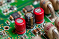
Voiding refers to the formation of air pockets under the solder joint, which can weaken the connection. In power electronics PCBA, voiding is particularly common in thermal pads and BGAs, where the large contact areas tend to trap air during the soldering process. Inadequate wetting on these large pads can further exacerbate the problem, as the solder fails to completely adhere to the pad, creating weak joints that affect thermal and electrical performance. Ensuring proper wetting is essential for reliable solder joints in power electronics assemblies.
Tombstoning, a phenomenon where one end of a component lifts off the PCB during soldering, is a common issue in power electronics PCBA. This is often caused by imbalanced heating or insufficient solder paste. Similarly, solder bridging (unwanted solder connections between adjacent leads) and insufficient solder joints (where there isn’t enough solder to form a reliable joint) are common issues that can occur due to inconsistent solder paste application or incorrect reflow profiles. These defects reduce the overall reliability of the product and increase the likelihood of failure.
Head-in-pillow (HiP) is another defect commonly observed in BGAs and is caused by poor solder ball wetting. This defect occurs when the solder ball fails to fully wet the pad, leaving the ball suspended over the pad like a "head in a pillow."
This condition reduces the strength of the connection and can lead to failure under stress. The presence of HiP can be particularly detrimental in high-reliability power electronics where robust connections are crucial for the stability of the system.
The reflow temperature profile plays a pivotal role in ensuring solder joint quality and minimizing defects. In power electronics PCBA, optimizing the temperature profile is critical due to the varying thermal mass of different components.
Choosing the right reflow oven is crucial to accommodate these needs.
The preheat stage must ensure uniform heating without stressing the components, while the soak phase allows for thermal uniformity before reaching the reflow peak. The cooling phase must be gradual to prevent thermal shock.
Balancing all these stages effectively ensures that high-power components experience minimal thermal stress while achieving high-quality solder joints.
With the growing use of lead-free solder, reflow temperature profiles need to be adjusted to accommodate the higher melting temperatures of these solders.
Selecting the right lead-free reflow oven is vital to meet these challenges. Additionally, high-density designs often feature components that are packed tightly together, further complicating the heating process.
To achieve consistent soldering results, profiles need to be tuned to account for the increased complexity of these designs.

Nitrogen reflow soldering has emerged as a valuable solution for power electronics PCBA due to its ability to reduce oxidation and improve solder wetting. The nitrogen environment prevents the formation of oxides on the components and solder pads, ensuring high-quality joints.
For power electronics with high-density components and critical performance requirements, nitrogen reflow provides enhanced reliability by improving solder joint consistency and reducing defects like voiding and head-in-pillow.
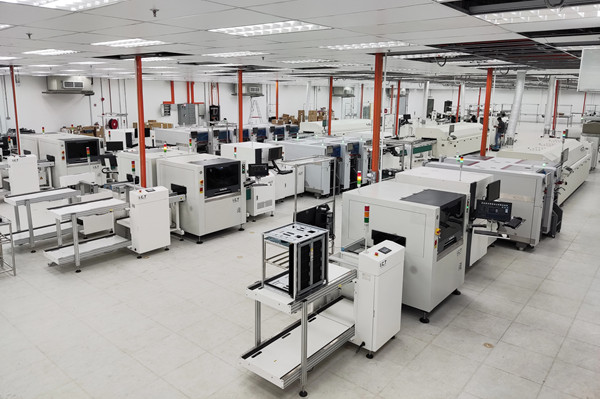
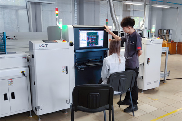
Solder Paste Inspection (SPI) and Automated Optical Inspection (AOI) play critical roles in defect prevention and real-time feedback during the reflow soldering process.
SPI ensures accurate solder paste application, while AOI detects defects such as tombstoning, bridging, and insufficient solder joints early in the process.
By integrating these inspection systems into the reflow process, manufacturers can minimize defects and improve the overall yield of power electronics PCBA.
Integrating reflow soldering with inline inspection systems such as SPI and AOI allows manufacturers to achieve real-time quality control. This integration not only ensures immediate detection of defects but also enables continuous process monitoring.
The real-time feedback allows operators to adjust the process promptly, reducing the chances of defects and improving overall production efficiency.
Incorporating real-time process monitoring and traceability systems into the reflow soldering process enhances process stability. Manufacturers can track every aspect of the production process, from solder paste application to final inspection.
This allows for continuous improvement, as operators can identify patterns, implement corrective actions, and prevent defects from reoccurring.

A case study of high-power inverter assemblies illustrates how warpage can affect component alignment and solder joint reliability. By optimizing temperature profiles and using controlled cooling stages, the company was able to significantly reduce warpage and achieve consistent solder joints. This resulted in improved product reliability and performance in high-power applications.
Another case study demonstrates how optimizing temperature profiles and integrating AOI systems led to improved yield in power electronics manufacturing. The company saw a significant reduction in defects such as voiding, bridging, and insufficient solder joints, resulting in higher production efficiency and lower rework costs.
As the demand for eco-friendly manufacturing processes grows, the electronics industry is exploring new materials that are both sustainable and effective in high-power applications.
Advances in materials, such as lead-free solder with enhanced performance, are changing the way reflow soldering is conducted, with a focus on reducing environmental impact while maintaining high reliability.
The use of AI-driven profiling systems is on the rise, offering more precise control over the reflow soldering process. AI systems can predict temperature fluctuations, adjust profiles in real-time, and improve overall production efficiency.
These innovations are driving the shift towards more sustainable and efficient manufacturing processes, ultimately contributing to the growth of power electronics.
In conclusion, reflow soldering in power electronics PCBA poses unique challenges, including thermal management, PCB warpage, and soldering defects. However, with advancements in temperature profile optimization, nitrogen reflow soldering, and automated inspection, manufacturers can overcome these challenges and improve product reliability. As the industry moves towards more eco-friendly processes and AI-driven profiling, the future of power electronics reflow soldering looks promising, with greater efficiency and sustainability on the horizon.
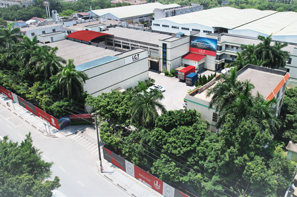
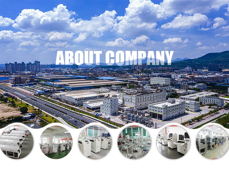
At I.C.T, we are committed to providing cutting-edge solutions and comprehensive support to help you achieve optimal reflow soldering results. Reach out to us today to learn how we can help streamline your power electronics production for enhanced reliability and efficiency.
What makes reflow soldering more challenging for power electronics PCBA compared to standard assemblies?
How can adjusting the temperature profile reduce voiding and warpage in power PCBA?
How does AOI help in detecting and preventing reflow defects in power electronics?
Is nitrogen reflow soldering worth the investment for high-reliability power PCBA?
How does I.C.T support manufacturers in overcoming these reflow challenges?