English
Views: 0 Author: Vinci Zhang Publish Time: 2026-10-12 Origin: Site


Warped boards are one of the quietest ways a reflow process fails. The board bends as it heats, the paste deposit and the component stop touching the way they should, and you end up with open joints, lifted corners, and poor contact that can pass visual inspection and still fail in the field. The good news is that warpage is largely predictable: it follows from material expansion mismatch, board geometry, absorbed moisture, how the board is supported in the oven, and how fast it is cooled. Get those five things under control and most warpage problems stop before they start.
This article is written for process engineers and line supervisors who have to keep large, thin, or dense boards flat through the thermal cycle. It covers what warpage looks like on the line, the cause families that drive it, the design and handling controls that prevent it, and the measurement and equipment choices that keep it from coming back. If you want the wider diagnostic method that this article fits into, our complete guide to reflow soldering defects explains how to classify any defect before you change a setting.

The single most useful thing to know about warpage is that it is a shape problem, not a solder problem. The alloy may be perfect and the paste may be perfect, but if the board is not flat when the solder melts, the joint forms under the wrong contact and the result is unreliable. Treat warpage as a board-condition defect first and a profile defect second.
Bow is the board curving like a shallow banana along its length or width. Twist is rotation around a diagonal, so one corner lifts while the opposite corner stays down. Both are out-of-flat deformation, and both get worse as the board crosses the peak of the thermal cycle.
You rarely see it by eye at the oven because the board is hot and moving. You see it after the fact as components that sit proud at one edge, solder fillets that are thin or missing at the board corners, and area-array packages whose outer balls never wetted. A board that springs flat again after cooling can still have left a row of opens behind.
A warped board changes the distance between the pad and the component termination, and that distance controls how much solder actually bridges the gap. At the center of a large BGA or LGA, a few tenths of a millimeter of bow can be enough to leave the corner balls touching paste but never wetting it. The joint looks formed and tests open later.
Warpage also moves the whole assembly relative to the conveyor and the reflow airflow. A board that rocks on its support points sees uneven heating, so a warpage problem quietly becomes a thermal problem as well. That is why the defect is worth fixing at the source rather than compensating with profile changes.
Every warpage case on a reflow line comes from one or more of these: material mismatch, board geometry, absorbed moisture, and inadequate support. Material mismatch is about how the laminate and copper expand at different rates. Geometry is about thickness, layer count, and how evenly copper is spread. Moisture is vapor pressure building inside the board as it heats. Support is about whether the conveyor and carriers hold the board flat while it softens.
Notice that three of the four are decided before the board reaches the oven. That is the theme of this article: most warpage is prevented upstream, and the oven profile is the last lever, not the first.
Warpage is a latency defect. A board can leave the oven looking acceptable, pass AOI on the visible parts, and still carry corner opens under a BGA that only show up under X-ray or in temperature-cycling test. Because the symptom is hidden, the cause is easy to misattribute to the package or the paste.
The practical defense is to measure flatness on a sample of real boards at temperature, not just at room temperature, and to trend it. If you only inspect cold boards, you will keep missing the warpage that happens only while the laminate is soft and hot.
The short answer is that different materials in the board expand by different amounts as they heat, and the board bows to relieve the stress. The longer answer is that the reflow cycle makes this worse at exactly the moment the board is softest, which is during the soak and peak stages.
Every material has a coefficient of thermal expansion, the rate at which it grows per degree of temperature rise. The copper foil on a board expands at a different rate than the fiberglass-and-resin laminate it is bonded to. When the assembly heats, those layers want to grow by different amounts, and the only way the bonded stack can respond is to curve.
This is the core mechanism behind nearly all reflow warpage. It does not require a defective board; it is built into the physics of a multi-material sandwich. What changes between boards is how strong the mismatch is and whether the design balances it.
A faster heat-up does not cause the mismatch, but it concentrates the stress into a shorter window. The board has less time to equalize and less time for the softened laminate to relax, so the peak bow is often sharper with a steep ramp than with a gentler one.
Slowing the ramp is not a cure, because the mismatch is still there at peak temperature. But a controlled ramp reduces the transient stress and gives the support system a better chance to hold the board. The ramp is a tuning knob, not a root-cause fix.
A thin board has less stiffness to resist the bending force from expansion mismatch. The same material imbalance that bows a 0.4 mm board mildly may bow a 1.6 mm board almost not at all. Board thickness is one of the strongest predictors of warpage risk, which is why thin consumer and flex-rigid designs are where this defect shows up most.
The counter is to add support, but support has limits. A very thin board still needs careful handling and sometimes a carrier, because edge-rail support alone may not be enough to keep it flat through peak.
Bow and twist share a cause but behave differently on the line. Bow lifts the board along one axis and tends to open joints at the two ends. Twist lifts one corner and tends to open joints at the corners and edges of large packages where the gap is largest.
Knowing which one you have changes the fix. Bow often points to symmetric imbalance in layer or copper distribution. Twist often points to an asymmetric layout or an asymmetric support path. The measurement section later explains how to tell them apart with a simple gauge.

Material mismatch is the family you can do the least about after the board is built and the most about before it is built. The lever is design and supplier choice; the line-side control is mostly support and profile.
Copper expands more per degree than the FR-4 laminate that carries it. In a balanced stack-up the copper on the top and bottom layers is roughly equal, so the bow from each side cancels. In an unbalanced stack-up, one side pulls harder than the other and the board bows toward the side with more copper or stiffer material.
This is why the bare board fab notes matter. A board that was fine as a bare substrate can still warp once copper and components are added, because the added material changes the balance.
More layers mean more chances for imbalance. A twelve-layer board with heavy planes on three layers and thin signal layers elsewhere can carry a strong internal bending moment that only shows up when the resin softens at reflow temperature.
Symmetry in the stack-up — matching copper weight and layer position top to bottom around the mid-plane — is the design rule that most reduces this. It is a design conversation, not a line adjustment, which is why this cause family belongs upstream.
Large packages such as BGAs, LGAs, and connectors act like local stiffeners. They resist bending where they sit and force the board to bend around them. The result is often maximum bow at the package corners, exactly where the joints are most exposed.
This is one reason head-in-pillow and corner opens cluster under big packages. The package holds its shape while the board bows away from it. A useful related read is our guide on cold solder joints, because an open driven by warpage can look like a cold or partial joint on the bench.
Lead-free SAC alloys such as SAC305 melt at a higher temperature than tin-lead, with a solidus around 217 degrees Celsius — confirm the exact value with the alloy supplier data sheet before you set a profile. That higher peak means the board spends more time near the temperature where its laminate is softest, which is the worst case for warpage.
The higher reflow temperature does not create the mismatch, but it widens the window in which the board is free to deform. Process control and support matter more on lead-free lines for exactly this reason. For a look at oven configurations built to hold tight windows on lead-free products, our overview of SMT reflow oven solutions groups them by application and process control.

Design is where warpage is cheapest to prevent, because a balanced board costs the same to fab as an unbalanced one and never needs a line workaround. The controls here are simple rules applied early.
The strongest single design rule is to distribute copper as evenly as possible, both within a layer and between the top and bottom of the stack. Heavy copper poured on one side and sparse on the other is an open invitation to bow.
When copper cannot be balanced for functional reasons, the next best move is to place balancing copper in unused areas so the expansion forces cancel. This is a layout decision, and it is far easier than fighting the resulting warp on the line later.
How a board sits in its panel affects warpage too. A board routed into a panel with uneven breakaway tabs, or one placed off-center in a large panel, can see uneven support and uneven heating that amplify the bow.
Panel design that keeps the board centered, with symmetric tooling strips and enough frame stiffness, reduces both the thermal and the mechanical contribution to warpage. It also makes conveyance steadier, which feeds directly into the support discussion.
You do not need an expensive simulation to avoid the worst warpage. Mirror the layer sequence around the mid-plane, match copper weights top to bottom where you can, and avoid putting all the heavy planes on one side. These three habits remove most of the avoidable material mismatch.
Where the product allows, specifying a slightly thicker core or a more symmetric laminate choice pays back on the line as fewer warpage escapes. The fab can usually advise on a balanced stack-up at no extra cost if you ask early.
Under a large BGA or LGA, pad design interacts with warpage. A non-solder-mask-defined pad array, or one with weak planarity, makes the corner-gap problem worse because the balls have less tolerance for the board lifting away.
Tighter placement accuracy also helps here, because a package already offset toward one corner has less margin before the bow opens a joint. Our guide on component shifting covers the placement and paste thresholds that keep large packages centered, which is a useful companion to the support work in the next sections.

Moisture is the one warpage amplifier that is entirely within your control on the line, and it is the one most often skipped under schedule pressure. A board or component that has absorbed water releases it as vapor at reflow temperature, and that internal pressure adds to the bow and can cause delamination.
Absorbed moisture does two things. It adds internal vapor pressure that pushes layers apart, and it weakens the resin so the board deforms more easily under the same expansion mismatch. The board that was flat when dry can bow or even delaminate once it is wet and hot.
Humidity and storage time are the variables. Boards left in unsealed packaging, or stored in a humid room, pick up moisture steadily. The defect pattern often tracks with the season or with a wet week, which is a useful clue when warpage appears without any process change.
The standard that defines how moisture-sensitive components are classified, packed, stored, and baked before reflow is IPC/JEDEC J-STD-020, published jointly by IPC and JEDEC. Following its moisture sensitivity classification tells you whether a bake is required and for how long before the parts see reflow heat.
Baking the board and the moisture-sensitive devices per that classification is the standard control, and it directly reduces the vapor pressure that contributes to warpage and popcorning. When warpage appears on a board that was otherwise well designed, a missing or inadequate bake is one of the first things to check.
The bake only works if the part is then protected. Once baked, a moisture-sensitive device has a floor life — a limited time it can sit exposed before it must be used or rebaked. Letting that clock run out in a humid room undoes the bake.
A simple, enforced storage routine beats heroic profile work every time. Sealed dry packs, a logged floor life, and a rebake step when the limit is exceeded keep moisture out of the equation. This is a discipline problem more than an engineering one.
Baking removes moisture but does nothing for material mismatch or poor support. If you bake a board and it still warps, the cause has moved to design, geometry, or conveyance, and you should stop reaching for the oven and look upstream and at the support hardware.
The useful habit is to confirm which family you are in before acting. Bake first if the history is missing; if the defect survives a proper bake, move to support and profile. Changing the temperature window to compensate for moisture you could have baked out is the wrong order.

Support is the line-side control that most directly fights warpage. The board is softest at peak temperature, and if the conveyor or carriers do not hold it flat then, it will take the shape of whatever is holding it.
During the soak and peak stages the laminate softens and loses stiffness. At that moment the board will conform to its support rather than hold its own flat shape. Edge rails that pinch only the edges of a large thin board let the middle sag; a carrier that cradles the whole board holds it flat.
Support is therefore not just about transport. It is the physical constraint that determines the final board shape at the moment the joints form. Get it wrong and no profile change will flatten the board.
Edge-rail conveyors are fine for small rigid boards but weak for large thin ones, because the unsupported span between rails bows. Finger conveyors and custom carriers that support the board across its width are the usual answer for panels and large boards.
The choice depends on the product. A carrier adds handling time and cost but can be the only way to hold a very thin or very large board flat through peak. For high-mix lines, adjustable rail supports and a small set of carriers cover most cases without a carrier per product.
A conveyor that is not flat, or rails that are not parallel and level, imposes its own warp on the board. The board follows the rail path, so a twisted rail line produces a twisted board even if the material is balanced.
Rail alignment and conveyor flatness belong in preventive maintenance, not in troubleshooting afterthoughts. A quick rail-level check at shift start catches the slow drift that turns a good process into a warpage-prone one. This is one of the cheapest checks with the highest payoff.
Thin and large boards need the most support and the gentlest handling. Edge rails plus a center support bar, or a full carrier, keeps the span from sagging. For flex and flex-rigid designs the support plan is part of the process definition, not an afterthought.
The sign of inadequate support is warpage that gets worse with board size but is absent on small boards run on the same profile. That pattern points straight at support rather than at the alloy or the paste.
The profile is the last lever, not the first, but it still matters. A well-designed profile reduces transient stress and avoids adding cooling shock on top of an already stressed board.
The only meaningful warpage measurement is on a real board with thermocouples attached, including at the locations where bow is worst — usually the corners of large packages and the board center. The oven display tells you the zone setting; it does not tell you the board shape.
A profiler that also captures board curvature, or a separate flatness check at peak, shows you whether the profile is helping or hurting. Without that measurement you are guessing about a defect you cannot see at the oven.
A soak stage that equalizes temperature across the board reduces local gradients that add to bow. An excessively long or hot soak, however, softens the laminate longer and can let support deficiencies show through. The soak is a balance, not a maximum.
Peak temperature should meet the alloy requirement without overshooting. Because lead-free peaks are already high, there is little room to trade temperature for flatness, which is another reason support and design do the heavy lifting and the profile only fine-tunes.
Cooling too fast can lock in stress and even add a reverse warp as the board contracts unevenly. Cooling too slowly lets the board sit soft and supported longer, which is usually safer for shape but can grow intermetallic layers if taken to extremes. A controlled, even cooling zone is the goal.
The updated cooling zone on modern ovens exists for exactly this reason: to bring the board down through the soft window evenly rather than shock it. Even cooling is better than fast cooling for warpage control.
Nitrogen mostly affects oxidation and wetting margin; it is not a warpage control. Running under nitrogen will not flatten a board, and it should not be bought to solve a warpage problem. Its place is on products where lead-free wetting margin is tight.
The discipline here is to use each control for its real purpose. Nitrogen for wetting, support for shape, design for balance, and bake for moisture. Mixing them up is how teams spend money on the wrong lever.
You cannot manage warpage you do not measure. This section covers how to see it, how to catch it on the line, and how equipment choice affects how much warpage you fight.
The standard line-side method is a flatness gauge or a three-point probe on a cooled board, plus a high-temperature measurement on a sample using a profiler with curvature capture or a dedicated warpage rig. Room-temperature checks catch permanent set; in-situ checks catch the transient bow that causes the opens.
Trend the numbers rather than pass-fail them. A board that is creeping from 0.3 percent bow to 0.6 percent bow over a month is telling you something a single limit will miss. The trend is the early warning.
AOI catches visible symptoms such as lifted corners and missing fillets, but it misses the opens under a BGA that warpage typically causes. X-ray at the right angle is the detection tool for those, and it is worth building into the inspection plan for large packages. The same X-ray view is how you separate a warpage-driven open from reducing BGA voiding work, because voiding under the same packages is a different failure with a different fix.
Visual inspection of the board edges and corners for gap under components is a cheap first check. If a large package rocks or shows a visible edge gap after reflow, assume warpage until measurement proves otherwise.
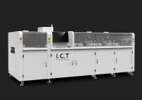
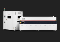
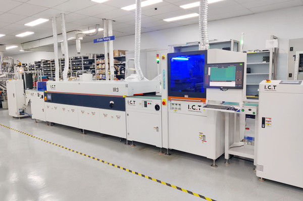
Equipment choices shape how much warpage you fight. More and better-controlled heating zones give a gentler, more uniform ramp and soak, which reduces transient stress. Reliable, flat conveyance and good rail alignment give the board a true reference plane. Controlled cooling avoids shock. For fine-pitch and lead-free work where the warpage window is tightest, a modular hot air reflow oven in the Lyra series — with a multi-zone heating chamber, a separate cooling stage, and optional nitrogen support — gives process engineers the zoning flexibility and consistent convection to hold a flat board through peak.
The question is not which machine has the longest spec sheet but which one matches your product mix. A line running large thin lead-free boards needs more zones and better support than one running small forgiving consumer assemblies. Match the equipment to the warpage risk.
Warpage is rarely solved by one change. It is solved by balancing design, bake discipline, support hardware, and profile together, which is exactly the kind of integrated view a turnkey line supplier can help with. I.C.T builds complete SMT turnkey lines, including the Lyra 622, 733, and 933 series reflow ovens with their different zone counts, plus factory planning, installation training, and overseas on-site technical support.
If you are chasing warpage on a difficult board, the fastest path is usually a joint look at the board construction and the profile data with a process engineer who can see both at once. The fix is almost always a combination of the controls in this article, applied in the right order: design and bake first, support second, profile last.
Warpage is out-of-flat deformation of the board as it heats, usually bow along one axis or twist around a diagonal. It happens because the laminate and copper expand at different rates and the board is softest at the peak of the thermal cycle. The result is open joints, lifted corners, and poor contact that can pass visual inspection.
Sometimes partially, but rarely completely. A gentler ramp and a controlled soak reduce transient stress, and even cooling avoids locking in reverse warp. The root causes — material mismatch, copper imbalance, moisture, and poor support — are not fixed by temperature. Treat the profile as the last lever after design, bake, and support are addressed.
Absorbed moisture turns to vapor inside the board at reflow temperature, adding internal pressure that pushes layers apart and weakening the resin so it deforms more easily. Baking moisture-sensitive boards and components per IPC/JEDEC J-STD-020 before reflow removes that pressure. A proper bake is one of the cheapest warpage controls available.
A thin board has less stiffness to resist the bending force from expansion mismatch, and a large board has a longer unsupported span that sags under its own softness at peak temperature. Both factors multiply the bow. Such boards need carriers or center support rather than edge rails alone.
Measure flatness on a cooled board with a gauge or three-point probe to catch permanent set, and measure a sample at temperature with a profiler that captures curvature or a dedicated warpage rig to catch the transient bow. Trend the numbers over time rather than relying on a single pass-fail limit, and use X-ray to find the hidden opens under large packages.
No. Nitrogen reduces oxidation and improves wetting margin for lead-free alloys, but it does not change the expansion mismatch or hold the board flat. Buy nitrogen for wetting, not for shape. Warpage is controlled with balanced design, moisture baking, proper support, and a controlled profile.