English
Views: 0 Author: Mark Publish Time: 2025-12-09 Origin: Site


In today's fast-paced SMT manufacturing world, a reliable Solder Paste Inspection Machine can make all the difference between high-quality PCB and costly rework. Whether you're running a small prototype line or a high-volume production facility, understanding SPI technology helps you catch solder paste defects early, boost your yield, and save money. This guide walks you through everything from basics to advanced integration, so you can decide if SPI fits your setup.

Solder paste inspection, or SPI, is a key step in surface mount technology (SMT) where a machine checks the solder paste printed on a PCB before components are placed. Think of solder paste as the glue that holds tiny parts like resistors and chips in place during soldering. If the paste is too much, too little, or in the wrong spot, it can cause big problems later, like short circuits or weak connections.
An SPI machine uses cameras and lights to scan the board and measure the paste. It looks for issues that the human eye might miss, especially on small boards with tiny pads. Without SPI, many defects slip through until final testing, wasting time and materials. According to industry reports, up to 70% of SMT defects start with bad solder paste printing. That's why SPI is like an early warning system for your production line.

In a typical SMT line, SPI comes right after the solder paste printer and before the pick-and-place machine. Here's how it fits in:
First, the printer applies solder paste to the PCB through a stencil. Then, the SPI machine inspects it immediately. If everything looks good, the board moves to placement where components are added. If not, the machine flags it for cleaning or reprinting.
This position is crucial because fixing paste issues early is much easier than after reflow soldering. In high-speed lines, SPI runs inline without slowing things down much. For smaller setups, offline SPI lets you check boards in batches. Either way, it prevents bad boards from going further, saving you from expensive scrap.
Skipping SPI might seem like a way to cut costs, but it often backfires. Industry data shows that without SPI, solder joint defects can account for 60-80% of total SMT failures. Each defective board might cost $10-50 in rework, not counting lost production time.
For example, in automotive or medical PCB manufacturing, a single bad solder joint could lead to product recalls costing thousands. A study by IPC, the electronics industry association, found that lines with SPI have 50% lower defect rates than those without. Over a year, that adds up to big savings. If your line produces 10,000 boards a month, even a 1% yield improvement could save $10,000 or more.

At its heart, an SPI machine works like a super-accurate scanner. It uses light and cameras to create a 3D map of the solder paste on your PCB. The main principle is called phase shift profilometry, where the machine projects patterns of light onto the board and measures how they distort over the paste deposits.
This light bounces back to the camera, and software calculates the height, width, and shape of each paste spot. It's similar to how your phone's face ID maps your features, but for tiny solder blobs. The machine compares this data to your design specs and flags anything out of tolerance.
SPI doesn't just take pictures; it measures specific things to ensure good soldering:
- Height: How tall the paste is. Too low means weak joints; too high can cause bridging.
- Area: The spread of paste on the pad. It should cover 80-100% without spilling over.
- Volume: The total amount of paste. This is crucial for consistent joints – aim for ±10% variation.
- Offset: If the paste is shifted from the pad center. Even 50 microns off can lead to tombstoning.
Some machines also check for shape defects like peaks or valleys in the paste. These measurements happen in microns, finer than a human hair, ensuring precision for modern tiny components.
When you run a board through SPI, here's what happens:
1. The conveyor moves the PCB into position.
2. The machine scans the board, projecting light patterns.
3. Cameras capture images from multiple angles.
4. Software builds a 3D model and analyzes each pad.
5. Results show on screen: green for good, red for bad, with details on what's wrong.
6. If it's good, the board moves on; if not, it might auto-clean or alert you.
On the screen, you'll see colorful 3D views of the paste, like a topo map. It's easy to spot issues and adjust your printer settings right away.

2D SPI uses basic cameras to look at the top view of solder paste. It measures area and position but can't tell height or volume accurately. It's like judging a cake's doneness by looks alone – you might miss if it's undercooked inside.
Limitations include missing height defects, false alarms from shadows, and slower speeds on complex boards. For simple PCBs with large pads, 2D might work, but for modern electronics, it's often not enough. Prices start around $30,000, but you get what you pay for in accuracy.
3D SPI adds depth measurement using lasers or structured light, giving a full picture of paste volume and shape. It catches more defects, like insufficient volume that looks okay from above.
Advantages: Higher accuracy (down to 0.67 microns), fewer false calls, and better data for process tweaks. It's essential for fine-pitch parts like 01005 chips. While more expensive ($80,000+), it pays off in higher yields. Most top factories use 3D now.
Here's a quick comparison:
| Feature | 2D SPI | 3D SPI |
|---|---|---|
| Accuracy | Good for area (10-20um) | Excellent for volume/height (1-5um) |
| Speed | Fast (0.5-1s/FOV) | Faster on modern machines (0.35s/FOV) |
| False Call Rate | Higher (5-10%) | Lower (1-3%) |
| Best For | Simple boards | Complex, high-reliability |
Choose based on your PCB complexity and budget.

Industry reports show that solder paste problems cause up to 30% of all defects in PCB assembly. Without SPI, these issues often go unnoticed until later stages, leading to more failures. But when you add SPI, it can cut pre-reflow defects by as much as 70%, according to SMTA studies.
This means fewer bad solder joints overall, with some factories seeing a 60-80% drop in soldering problems. For example, a report from Global SMT says nearly 30% of PCBA defects come from poor solder paste, and SPI stops them early. In high-volume lines, this reduction can boost your overall yield from 90% to 98% or higher.
Think about it: if your line makes 10,000 boards a month, cutting defects by 60% could save hundreds of boards from scrap. Plus, SPI gives you data to fix printing issues fast, preventing repeat mistakes. Over time, this leads to more consistent production and happier customers. Remember, these numbers come from real industry data, so SPI isn't just a nice-to-have—it's a smart investment for better quality.
In one factory making phone parts, before SPI, they had a 5% rework rate due to solder issues. After adding SPI, defects dropped to under 1%, saving $200,000 in just six months.
This happened because SPI caught paste volume problems early, before they became hard-to-fix joints. Another example from a PCB manufacturer: their first-pass yield was stuck at 80%, with many printing errors.
Once they implemented SPI, yield jumped to 95%, and they reduced scrap by 50%. They used the machine's data to tweak their printer settings, like adjusting pressure and speed. In a study by Circuit Insight, a company saw a 70% reduction in defects after SPI, going from frequent bridges to almost none.
For a medical device maker, SPI helped meet strict quality rules, cutting failures from 2% to 0.5%. These cases show how SPI pays off quickly, often in under a year. If your factory faces similar issues, a simple trial could show big improvements right away.
Beyond just fewer defects, SPI cuts down on rework, which can cost $5 to $20 per board in time and materials. By catching problems early, you avoid pulling boards off the line later, saving hours of labor.
This leads to a higher first-pass yield, meaning more boards pass on the first try without fixes. For instance, factories report yields rising from 90% to 98%, which means less waste and faster output. SPI also gives you real data, like paste volume trends, so you can prevent issues before they start.
Over a month, this could save thousands in scrap costs alone. Plus, better quality means fewer returns from customers, building your reputation. Hidden perks include less downtime, as your team spends less time troubleshooting.
In the long run, SPI helps your whole line run smoother and more efficiently. It's like having an extra set of eyes that pays for itself through savings.

SPI looks at solder paste before parts are placed, so it spots issues like too little paste that could cause open joints later. AOI inspection Machine can't see under components, so it misses these hidden paste problems.
For example, if the paste volume is off by 20%, SPI flags it right away, but AOI only sees the bad solder after heating. SPI also checks height and shape, preventing bridges or weak spots that AOI might overlook.
In fine-pitch boards, SPI catches offsets as small as 50 microns, which AOI can't detect pre-reflow. This early catch saves you from costly fixes down the line. Studies show SPI handles 60-70% of print defects that AOI never sees.
Without SPI, many issues slip through to final testing. So, if paste is your weak spot, SPI is key to stopping them first. Overall, SPI focuses on prevention, while AOI is more about checking the end result.
AOI inspects after parts are placed and soldered, so it finds missing components that SPI can't see since it only looks at paste. For instance, if a chip is upside down or wrong polarity, AOI catches it easily. SPI misses post-print issues like shifted parts during placement.
AOI also spots surface scratches or dimensional errors on the finished board. In soldering, AOI detects bridges or insufficient solder after reflow, which SPI can't predict fully. Things like tombstoning, where parts stand up, are AOI's strength.
Data shows AOI covers 50% of assembly defects that happen after paste. Without AOI, you might ship boards with visible flaws. So, AOI is great for final checks, while SPI is for early paste fixes. Together, they cover the whole process.
For high-volume lines making over 10,000 boards a day, use both SPI and AOI inline for real-time checks. This keeps defects low and meets strict PPM goals. Start with SPI after printing to fix paste, then AOI after reflow for final assembly.
In medium-volume setups, like 1,000-5,000 boards, try offline SPI with inline AOI to save costs. This way, you batch-check paste but catch placement issues on the fly. For low-volume or prototype lines under 500 boards, begin with just SPI if paste is the main problem, adding AOI later if needed.
Budget tip: If money is tight, prioritize SPI since it stops 60% of defects early. Integrate them with smart software for data sharing, optimizing the whole line. Studies show using both boosts yield by 15-20% over one alone. Adjust based on your PCB complexity—more complex means both are essential. This combo ensures quality without slowing production.
")
If your PCB uses very small parts like 01005 resistors, 0201 capacitors, or 0.3 mm pitch BGA chips, you must have SPI. These tiny pads are only 0.15–0.25 mm wide, so even a 30-micron shift or 10 % volume error can cause open joints or shorts.
Human eyes and simple 2D printer cameras cannot catch such small mistakes reliably. A real factory example: one company making 5G modules used to get 8 % open joints on 0201 parts; after adding 3D SPI, that dropped to 0.3 %.
With fine-pitch, solder paste volume needs to stay within ±10 %, and only 3D SPI can measure that accurately every time. If you are moving to smaller packages to save space or add more functions, SPI becomes non-negotiable.
Without it, your yield will drop quickly and rework will become impossible on such tiny parts. In short, the smaller the component, the bigger the need for SPI.
Products for cars, medical devices, and airplanes must work perfectly because a failure can hurt people or cost millions. Standards like IATF 16949 (automotive) and ISO 13485 (medical) require full process traceability and very low defect rates, often below 50 PPM.
SPI gives you exact volume, height, and position data for every single pad, so you can prove to auditors that printing was correct. One automotive Tier-1 supplier reduced field returns from 1 200 PPM to 80 PPM just by adding SPI and closed-loop feedback to the printer.
In medical pacemakers or aerospace avionics, even one cold solder joint is unacceptable. SPI also creates a digital record of every board, which is needed for lot traceability. If your customer asks for CpK > 1.67 on solder paste volume, only SPI can deliver that data. Bottom line: when safety and certification are on the line, skipping SPI is not an option.
When your factory makes more than 5 000–10 000 boards per day and your customer wants less than 500 PPM (or even 100 PPM), manual checks or printer built-in 2D inspection simply cannot keep up.
At that speed, one bad print can create hundreds of defective boards in minutes. SPI inspects every board in 0.35–0.5 seconds and automatically stops the line or diverts bad boards.
A large smartphone ODM reported that adding SPI cut their printing-related escapes from 1 800 PPM to under 200 PPM while running 120 000 boards per day. The machine also feeds real-time data back to the printer to auto-correct stencil alignment and pressure.
In high-volume lines, the cost of one hour of rework can easily pay for a whole SPI machine. If you are chasing single-digit PPM levels, SPI is the only realistic way to get there consistently.
You know you need SPI when you see these warning signs: first-pass yield stuck below 96–97 % for months, most defects traced back to insufficient or excess solder paste, frequent bridging or open joints on fine-pitch parts, printer operators spending hours doing manual 2D checks, high rework cost after reflow, customer complaints about cold joints or field failures, CpK on paste volume below 1.33, or your process engineer says “we’ve tuned the printer as far as it can go.”
When these happen, you have reached the natural limit of a printer-only process. Adding SPI usually gives an immediate 3–8 % yield jump and lets you push the process much further. Many factories only realize this after a big quality incident. Don’t wait for that—look at your defect Pareto chart; if printing is always in the top three, it’s time for SPI.
")
If your boards are for toys, LED lighting, power supplies, or home appliances with component pitch 0.8 mm, 1.27 mm, or larger (like SOIC, 1206 resistors, big connectors), printing defects are easy to see with the naked eye or a cheap microscope.
These big pads forgive small volume errors, so even ±30 % paste variation usually solders fine. Many factories making simple double-sided boards with through-hole + a few SMD parts run perfectly for years using only a good printer with automatic vision alignment and regular stencil cleaning.
Rework is simple and cheap on these boards. As long as your defect rate stays below 1–2 % and customers are happy, you can skip dedicated SPI and save the $80 000–$150 000 investment. Just keep good printer maintenance and train operators well—that is usually enough for low-cost, large-pitch products.
When you produce fewer than 500–1 000 boards per week (common for prototypes, small-batch industrial controls, or custom orders), the cost of an SPI machine is hard to justify. One SPI costs the same as 6–18 months of an engineer’s salary.
In low-volume shops, engineers can manually check every board under a microscope after printing, clean bad ones, and reprint if needed. This takes only a few extra minutes per board. Many NPI (new product introduction) departments run successfully this way for years.
The risk is low because total scrap cost is small even if a few boards fail. Once the product moves to medium or high volume, you can add SPI later. For pure prototype or very low-volume lines, human inspection plus a good printer is still the most economical choice in 2025.
Instead of buying SPI, you can get surprisingly good results with these cheaper methods:
-Use a modern printer with strong APC (Automatic Position Correction) and built-in 2D vision—many DEK, GKG, or I.C.T printers can auto-correct stencil position to within 10–15 μm;
-Clean the stencil underside every 5–10 boards to prevent excess paste; perform regular manual 2D checks with a cheap USB microscope ($200–$500);
-Print a test board at the start of each shift and measure a few pads with a low-cost laser height gauge;
-Keep detailed printer logs and adjust squeegee pressure/speed based on trend charts.
Factories making simple boards report defect rates below 1 % using only these steps. Total extra cost is under $5 000 instead of $100 000+ for SPI. These alternatives work perfectly until you hit the limits described in chapter 6—then it’s time to upgrade.

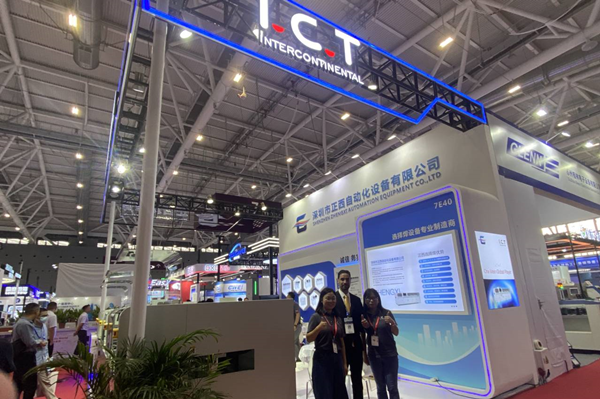
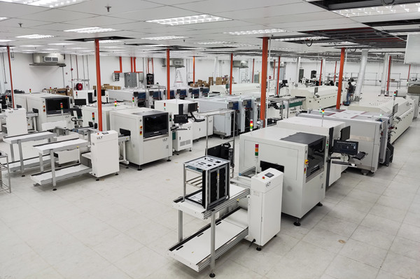
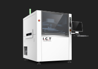
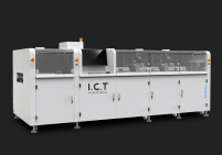
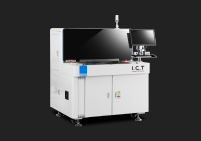
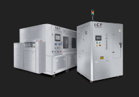
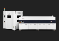
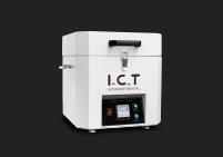
I.C.T currently offers several online 3D SPI models to fit different production needs. The most popular are the standard single-lane I.C.T-S510 series (60 × 50 mm to 510 × 510 mm boards), the upgraded I.C.T-S1200 that handles extra-large panels up to 1200 × 550 mm, and the high-speed dual-lane I.C.T-S510D that lets two printers feed one SPI at the same time.
All models share the same core 3D measurement technology but differ in board size, conveyor lanes, and throughput. For most customers starting their first SPI, the S510 or S1200 is the best choice because they are easy to install and cover 95 % of common PCB sizes.
If you already run two printers and want to save floor space, the dual-lane S510D can increase inspection capacity by almost 100 % without buying a second machine. Every model comes standard with automatic conveyor width adjustment, so changing products takes only seconds.

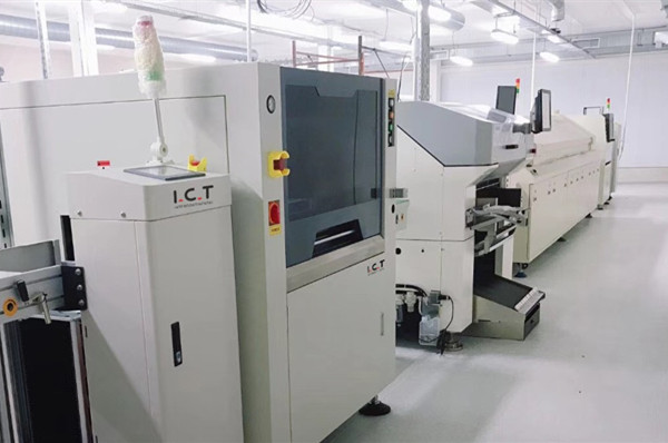
I.C.T 3D SPI completely eliminates shadow and random reflection problems that trouble older machines.
It does this by projecting programmable black-and-white moiré fringes from multiple directions and using a professional telecentric lens, so even shiny solder paste or dark PCB substrates give perfect images every time.
The standard camera is 5 million pixels with a true measurement accuracy of 0.67 μm; an optional 12 million-pixel camera is available for ultra-fine-pitch work below 0.3 mm.
Cycle time is only 0.35–0.5 seconds per field of view, meaning the machine easily keeps up with modern high-speed printers running 8–12 seconds per board. Multi-direction 3D projection also means almost zero false calls caused by component shadows or stencil aperture walls.
In daily use, operators report false alarm rates below 1 %, which saves a huge amount of review time compared with 5–10 % on ordinary machines.

You have two simple ways to program a new board.
First, import the Gerber or ODB++ files directly – the software automatically creates the inspection program in 5–10 minutes.
Second, if you don’t have Gerber data, just scan a golden board and the machine learns the correct pad positions and tolerances in one click.
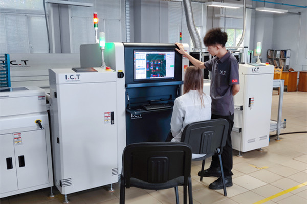
Both methods support offline programming, so you never stop the line while teaching a new product. The user interface is divided into operator level (simple pass/fail view) and engineer level (full data analysis and parameter tuning), so new workers can run it safely from day one while experienced engineers still get all the detailed statistics they need.
Real-time SPC charts, volume/height/area trend graphs, and defect heat-maps are all built in and update automatically.

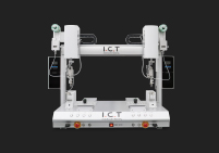
The whole machine uses an arch-bridge suspension structure with X/Y axes driven by independent high-precision servo motors and linear rails, exactly the same design used in high-end pick-and-place machines.
The base is a one-piece heavy cast frame that weighs over 800 kg, so vibration is almost zero even when the line runs at full speed. Slide positioning uses ball-screw + servo motor to keep the camera perfectly stable before and after movement.
All moving parts are protected by flexible closed-tank cable chains, so dust and solder paste particles never enter the motion system. These mechanical choices give I.C.T SPI repeatability better than 1 μm over years of 7 × 24 operation.
Many customers report that after three years they still pass factory calibration with the original glass plate – no expensive annual service contracts needed.
Every I.C.T SPI comes standard with automatic conveyor width adjustment, barcode reader interface, closed-loop feedback to most printer brands (DEK, GKG, Panasonic, Yamaha, Fuji, etc.), full SPC package, and NG board buffer.
Popular options include 12 M-pixel camera for 01005 components, dual-lane conveyor for the S510D model, tower light, UPS power backup, and MES/CFX/Hermes communication modules.
The machine runs on normal 220 V single-phase power and needs only 5–6 bar clean dry air, so installation is usually finished in one day. Because everything is modular, you can start with a basic model today and upgrade camera or software later without buying a new machine. This flexibility makes I.C.T very popular with factories that plan to grow step by step.
1. Speed: Match your line takt time.
2. Accuracy: 1um for fine-pitch.
3. Software: Easy programming, Gerber import.
4. Integration: MES, printer feedback.
5. Size: Fit your PCBs.
6. Camera: 5M+ for detail.
7. Service: Local support.
8. Price: Balance with ROI.
- PCB specs
- Volume needs
- Budget
- Required features
- Demo request
If SPI saves 2% defects on 100k boards/year at $20/board, that's $40k saved. Machine $100k pays back in 2.5 years, often faster.
1. Camera blur: Clean lens daily.
2. Conveyor jam: Check sensors weekly.
3. Light failure: Replace bulbs yearly.
4. Software crash: Update regularly.
5. Accuracy drift: Calibrate monthly.
Daily: Clean exterior, check alignments.
Weekly: Inspect belts, lubricate rails.
Monthly: Full calibration, backup data.
Keep machine in clean, temp-controlled room. Use covers when off. Avoid overloads.

Closed-loop sends SPI data back to adjust printer automatically, fixing issues in real-time for consistent quality.
CFX for plug-and-play, Hermes for board tracking, SECS/GEM for fab-wide control. These make integration easy.
Monitor trends, predict maintenance, trace defects. Boosts efficiency 20-30%.