English
Views: 0 Author: Site Editor Publish Time: 2025-12-25 Origin: Site


In modern SMT manufacturing, most quality problems do not originate at component placement or reflow. They begin much earlier—at the solder paste printing stage. Solder paste inspection defects are often the first visible signals that an SMT process is drifting out of control, even when downstream processes still appear stable.
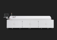
Solder Paste Inspection (SPI) plays a unique role in SMT lines because it is the earliest fully quantitative quality gate. Unlike AOI or functional testing, which detect defects after value has already been added to the board, SPI evaluates whether the foundation of the assembly process is correct before components are placed. When solder paste inspection defects are ignored or misinterpreted, manufacturers often experience a cascade of downstream issues such as tombstoning, insufficient solder joints, solder bridging, and BGA voids.
In high-reliability electronics manufacturing, SPI is no longer treated as a simple inspection step. Automotive, industrial, and EMS manufacturers increasingly use solder paste inspection defects as leading indicators of yield performance, rather than waiting for failures at AOI or functional test. This shift reflects a broader move toward data-driven SMT process control.
To fully understand why solder paste inspection defects occur—and why they are so critical—it is essential to first understand how solder paste inspection machines work across modern SMT production lines. A clear understanding of SPI principles, measurement logic, and system integration helps explain why many defects originate at the printing stage rather than later in the process.
This article focuses on the most common solder paste inspection defects in SMT, explains their root causes, and—most importantly—provides practical methods to fix them in real production environments.

Solder paste inspection defects refer to deviations detected during SPI measurement that indicate improper solder paste deposition on PCB pads. These deviations are not limited to obvious printing failures. In practice, many SPI defects fall within tolerance limits yet still pose a serious risk to long-term yield and reliability.
Typical SPI parameters include solder paste volume, height, area, offset, and shape consistency. A defect may be flagged when any of these parameters deviates from the expected baseline or shows abnormal variation across multiple boards. Importantly, SPI defects should be viewed as process indicators rather than simple pass-or-fail results.
For example, a gradual reduction in paste volume across a production run may not immediately trigger NG alarms. However, it often signals stencil clogging, solder paste degradation, or unstable printing parameters. Treating SPI as a statistical and trend-based tool is essential for effective defect control.
The solder paste printing process determines the amount and geometry of solder available for each joint. Once components are placed and reflowed, it becomes impossible to add solder where it is missing or remove solder where it is excessive without rework.
As a result, SPI defects are among the earliest and most accurate indicators of yield loss. Insufficient solder paste leads to weak joints or opens, excessive paste increases the risk of bridging, and paste misalignment causes non-wet or head-in-pillow defects—especially on fine-pitch and BGA packages.
From both quality and cost perspectives, correcting issues at the SPI stage is far more efficient than fixing defects after reflow. A single SPI-driven adjustment can prevent dozens of downstream defects.

This section outlines the most frequently encountered solder paste inspection defects, focusing on how they appear in SPI data, why they occur, and what risks they introduce.
Insufficient solder paste is one of the most common and most critical SPI defects. In SPI systems, it typically appears as low volume, reduced height, or incomplete aperture fill.
Common root causes include improper stencil thickness, clogged or worn apertures, insufficient squeegee pressure, and degraded solder paste activity. Environmental factors such as low humidity or improper paste storage conditions can further worsen the issue.
From an SPI perspective, insufficient paste often presents as a consistent downward trend rather than random failures. When left uncorrected, it leads directly to open joints, weak solder connections, and functional test failures.
Excess solder paste may appear less risky than insufficient paste, but it often results in more severe defects. SPI identifies excess paste through increased volume and height measurements, sometimes accompanied by distorted paste shapes.
Excess solder paste is commonly caused by oversized stencil apertures, excessive squeegee pressure, or paste slump. In high-density designs, even minor volume excess can significantly increase the risk of solder bridging during reflow.
SPI data enables engineers to distinguish between localized excess caused by aperture design and systemic excess caused by printing parameters—something that visual inspection alone cannot reliably achieve.
Solder paste offset occurs when paste deposits are misaligned relative to PCB pads. SPI systems detect this defect through X-Y offset analysis and centroid deviation measurements.
Typical causes include inaccurate board alignment, stencil shift, unstable clamping, or PCB warpage. In fine-pitch and micro-BGA applications, even small offsets can result in uneven solder collapse or insufficient wetting.
SPI is particularly valuable here because it can distinguish true misalignment from visual illusions that may appear acceptable to operators on the shop floor.
Smearing and shape deformation defects are often underestimated because they do not always trigger volume-based alarms. SPI systems detect these issues by analyzing paste geometry, edge definition, and height distribution.
Common causes include incorrect squeegee angle, excessive printing speed, poor paste rheology, or contaminated stencils. These defects frequently result in inconsistent solder wetting and unpredictable solder spread during reflow.
Many solder paste inspection defects are difficult to judge by eye. A deposit may appear visually acceptable yet still fall outside stable process limits when measured quantitatively.
This is why SPI alarms are sometimes dismissed as “too sensitive.” In reality, SPI does not detect defects earlier because it is stricter—it detects them earlier because it measures what the human eye cannot. Understanding this difference is critical for effective SPI adoption.

Stencil design has a direct and measurable impact on solder paste transfer efficiency. Aperture size, shape, wall finish, and area ratio all influence how consistently paste is released.
Poor stencil design often results in systematic SPI defects such as low volume or high variation across pads. SPI data provides objective feedback that helps engineers validate stencil designs before defects propagate into mass production.
Solder paste properties such as viscosity, metal content, and flux activity play a major role in printing performance. Improper storage temperature, insufficient warm-up time, or excessive open time frequently lead to SPI defects.
Material-related issues often appear in SPI as increased variation rather than sudden failures. Without SPI trend analysis, these problems are frequently misdiagnosed as equipment issues.
Key printing parameters include squeegee pressure, printing speed, separation speed, and snap-off distance. Each parameter affects paste deposition differently.
SPI enables engineers to optimize these parameters based on quantitative data rather than trial-and-error. When adjustments are guided by SPI trends, defect rates drop significantly and process stability improves.

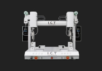
Modern SPI systems use 3D measurement technology to evaluate solder paste volume, height, and area. Volume is typically the most critical metric because it correlates directly with solder joint formation.
Height and area measurements provide additional insight into paste distribution and shape consistency. Together, these metrics form a complete picture of paste quality that cannot be achieved through 2D inspection.
Not every SPI alarm represents a true process issue. False calls often result from improper baseline setup, inconsistent reference boards, or tolerance settings that are too aggressive for the actual process capability.
Understanding the SPI inspection process in SMT lines is essential for distinguishing real defects from measurement noise. A structured SPI setup—covering golden board validation, baseline definition, and SPC-based trend monitoring—ensures that SPI functions as a reliable process control tool rather than a source of unnecessary alarms.
One common mistake is treating SPI as a defect-hunting system instead of a baseline-building mechanism. Stable SMT lines are not defined by the absence of alarms, but by consistent data distributions and predictable process behavior.

Correcting SPI defects begins with controlled, data-driven process adjustments. Changes to squeegee pressure, printing speed, or separation parameters should be guided by SPI trends rather than isolated alarms.
Incremental adjustments followed by immediate SPI verification allow engineers to confirm improvements before defects propagate downstream.
Equipment stability is essential for accurate SPI results. Printer alignment accuracy, stencil mounting repeatability, and SPI calibration all influence inspection reliability.
Regular calibration and preventive maintenance ensure that SPI data reflects true process conditions rather than equipment drift.
Preventive strategies include routine stencil cleaning, controlled solder paste handling, and continuous SPI trend monitoring. When SPI is integrated into preventive maintenance planning, defect recurrence drops significantly.
SPI data can be correlated with AOI and X-ray results to establish predictive quality models. For example, consistent low paste volume on BGA pads often correlates with voiding or head-in-pillow defects detected after reflow.
In advanced SMT lines, SPI feedback is used to trigger corrective actions or preventive maintenance before defects appear downstream. This closed-loop approach transforms SPI from a passive inspection tool into an active process control system.
Across multiple SMT production environments, manufacturers have achieved measurable yield improvements by restructuring their SPI strategy. By optimizing SPI placement, refining parameters, and training operators to interpret data correctly, defect rates were reduced without increasing inspection time.
These cases demonstrate that SPI effectiveness depends more on system integration and process understanding than on individual machine specifications.

The location of SPI within the SMT line determines which defects can be detected early and corrected efficiently. Proper SPI placement minimizes rework and improves overall process stability.
High-mix, low-volume production requires flexible SPI programming, while high-volume and automotive lines prioritize stability and data consistency. Selecting SPI capability based on production requirements is essential for long-term success.
")
Controlling solder paste inspection defects is not about adding more inspection steps—it is about designing the SMT line so defects are prevented, detected early, and corrected systematically.
I.C.T approaches SPI from a full SMT line perspective rather than treating it as a standalone machine. During SMT line planning, I.C.T evaluates product type, component density, production volume, and quality targets to determine how SPI should interact with printers, placement machines, and downstream inspection systems.
Beyond equipment selection, I.C.T supports customers with process setup, SPI parameter definition, and operator training. This ensures SPI data is correctly interpreted and used for process optimization instead of generating unnecessary false calls.
By helping manufacturers treat SPI as a decision-making tool rather than a simple inspection gate, I.C.T enables customers to transform solder paste inspection defects into actionable insights that improve overall SMT line stability.
Solder paste inspection defects are not merely inspection results—they are early warnings of process instability. When properly understood and managed, SPI becomes one of the most powerful tools for improving yield and reliability in SMT manufacturing.
By focusing on root causes, leveraging SPI feedback, and integrating inspection into a closed-loop quality strategy, manufacturers can move from reactive defect correction to proactive process control. For manufacturers seeking stable and scalable SMT production, controlling solder paste inspection defects is one of the most effective starting points.
1. What is the most common solder paste inspection defect?
Insufficient solder paste is the most frequently observed SPI defect and a leading cause of open solder joints.
2. Can SPI eliminate soldering defects entirely?
SPI cannot eliminate defects on its own, but it significantly reduces defect rates when used as part of a closed-loop process.
3. How often should SPI parameters be reviewed?
SPI parameters should be reviewed whenever materials, designs, or environmental conditions change.
4. Is SPI necessary for low-volume SMT production?
Yes. Even in low-volume production, SPI provides valuable insight into process stability and helps prevent costly rework.
If you are planning a new SMT line or looking to stabilize an existing process, a well-designed SPI strategy is often the fastest way to reduce defects—feel free to discuss your application with the I.C.T team.