English
Views: 0 Author: Site Editor Publish Time: 2025-11-21 Origin: Site


As component sizes shrink to the 008004 level, the internal world of a circuit board becomes more intricate than a strand of hair.
The more precise electronics become, the easier it is for fatal problems to hide where they cannot be seen.
These “latent defects” are causing repeated, hard-to-explain field failures in high-reliability sectors such as automotive, medical, aerospace, and 5G.
AOI cannot see them.
ICT cannot detect them.
Manual inspection has no chance at all.
Understanding X-ray Inspection properties and standards is therefore no longer optional—it is the foundation for evaluating what can truly be detected, measured, and trusted inside modern solder joints.
Only high-resolution X-ray inspection can non-destructively reveal voids, bridging, head-on-pillow, poor wetting, insufficient solder fill, wire-bond issues, and other deep-level defects—just like a true “through-view”.
It is currently the only inspection method capable of providing a truly reliable assessment of solder-joint quality.

The most dangerous problems on modern PCBs are often completely invisible to the naked eye.
Voids, bridging, cold solder joints, and head-in-pillow defects act like “latent time bombs,” triggering random failures.
On high-density PCBs, these issues become unavoidable.
Today`s BGA packages feature pitches as small as 0.35 mm.
Large thermal pads on QFN and LGA packages increase the risk of hidden defects.
Stacked packages such as PoP and SiP multiply the number of solder joints dramatically.
Even hash boards for cryptocurrency miners may contain thousands of entirely invisible solder joints.
The risks scale accordingly:
Solder ball voiding exceeding 25%.
Hidden bridging beneath QFN thermal pads.
HiP (Head-in-Pillow) defects caused by package warpage.
Cold joints and poor wetting due to ENIG/OSP surface finishes.
Insufficient barrel fill and circumferential cracks in PTH vias.
Wire bond cracks or bond lift-off inside semiconductor packages.
These are all “unseen but catastrophic” defects that can cause complete device failure.
No matter how advanced AOI becomes, it can only see the surface.
Even the most sophisticated 3D AOI can analyze only external solder fillets and surface geometry.
Real defects hide beneath component packages, inside solder joints, and under thermal pads.
ICT can check electrical continuity but cannot detect voids, cracks, or mechanical defects inside solder joints.
Many joints appear “electrically fine” during testing, yet fail completely after 500–1000 thermal cycles.
This is where the danger lies—the surface looks normal, but the internal failure countdown has already begun.
Automotive ISO 26262 ASIL-D.
IPC-7095 Level-3 BGA requirements.
Aerospace DO-160.
Military MIL-STD-883.
These standards increasingly mandate 100% X-ray inspection for hidden solder joints in safety-critical components.
Automotive ECUs, medical implants, flight-control electronics, aerospace systems, and 5G base stations—none of these industries can tolerate invisible risks.
High-reliability inspection is no longer optional—it has become the manufacturing baseline.
To detect hidden solder joint defects, one must first understand how X-rays “see through” a PCB.
X-rays in the 50–160 kV range pass through the PCB.
Different materials absorb radiation differently:
Solder: highest density, darkest in the image
Copper and silicon: intermediate absorption, gray
FR-4 and air: least absorption, brightest
2D imaging provides a top-down view.
2.5D adds a 60° oblique viewing angle and stage rotation to observe hidden structures from the side.
True 3D CT reconstructs the entire solder joint into volumetric data with voxel resolution as fine as 1 µm—essentially “slicing” the solder joint layer by layer for precise analysis.
Transmission mode is fastest, ideal for in-line sampling.
Oblique viewing (45°–60°) separates overlapping BGA rows and reveals QFN bridging.
For failure analysis—such as void volume measurement or crack propagation—CT is essential.
3D CT results show exactly what is happening inside the solder joint, removing guesswork.
Equipment—not X-ray technology—is the limiting factor for clear imaging.
Critical parameters include:
Tube voltage stability
Focal spot size (<1 µm)
Detector pixel pitch
Geometric magnification (up to 2000×)
Thermal stability of the sealed-tube X-ray source
These determine whether fine internal cracks, micro-voids, and other subtle defects are visible.

Voids inside BGA/CSP solder balls can reduce thermal conductivity by up to 40% when the void ratio exceeds 25%.
Automotive OEMs often require total void ratio <15% for powertrain and ADAS modules.
A drone or EV control board with such voids would operate at risk—the margin for safety is zero.
Excess solder paste under thermal pads can form invisible shorts.
During vibration or thermal cycling, these shorts grow, eventually causing catastrophic failure.
QFN and LGA packages appear perfect externally, but may hide danger internally.
HiP defects form “mushroom” or “Saturn ring” shapes.
Their mechanical strength is nearly zero and can fail under minimal stress.
X-ray imaging reveals these internal structures early, long before failure occurs.
Insufficient PTH solder fill, cracks, wire sweep, or delamination compromise reliability.
X-ray verifies PTH fill rates (75%–100%) and detects hidden defects immediately.
High-reliability industries mandate 100% X-ray inspection to identify these unseen “time bombs.”
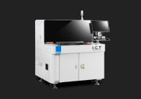
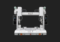
Choosing an X-ray system is about matching the tool to your application.
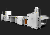
Offline systems offer 1–2 µm resolution, 60° tilt, 360° rotation, and full CT scanning.
Ideal for automotive, medical, and NPI industries—where reliability is critical.
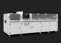
Inline systems trade some resolution for speed.
Perfect for high-volume consumer electronics, improving throughput.

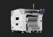
High-end market leaders: Nikon XT V, YXLON Cheetah EVO, Nordson DAGE Quadra, and Viscom.
I.C.T has emerged as the fastest-growing brand globally, offering equal or superior performance at 40%–60% lower cost, with innovative bilingual software.
For companies seeking a balance between quality and cost, I.C.T is a top choice.
Use carbon-fiber fixtures to stabilize PCBs.
Dedicated programs for each package type:
BGA: 45° oblique
QFN: 0° transmission
Semiconductor: high-mag gold wire
Tailored programming improves accuracy and reduces false positives.
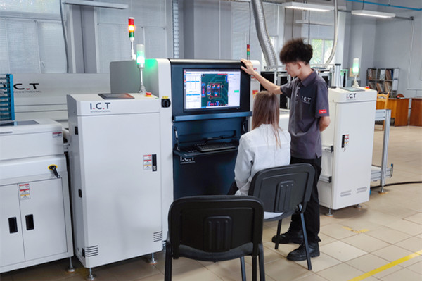
I.C.T software calculates void %, bridge thickness, barrel fill %, and generates compliant pass/fail reports.
Ensures inspections meet global quality and reliability standards.
Hidden solder joint defects cause over 70% of field failures in high-reliability electronics.
Only X-ray inspection can reliably detect them.
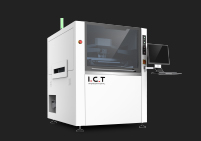
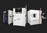
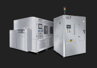
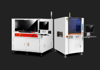
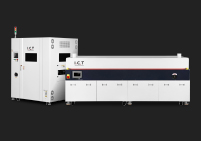
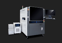
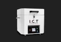
I.C.T X-7100, X-7900, and X-9200 deliver sub-micron resolution, intelligent software, and global service.
They help factories reduce escape rates below 50 ppm and achieve ROI in under 8 months.
Choosing the right X-ray solution is about safeguarding performance, reliability, and brand reputation.
1. What void percentage is acceptable in automotive BGA?
IPC-7095 Class 3: ≤25% total, no single void >15%.
Most Tier-1 suppliers now require ≤15% total and ≤10% single void for critical joints.
2. Can X-ray replace AOI completely?
No. Best practice: SPI + 3D AOI + X-ray for near-zero escape.
3. What is the typical ROI?
4–8 months, through avoided recalls, reduced warranty costs, and eliminated manual inspection labor.
4. How to choose between ICT models?
X-7100: general PCBA
X-7900: semiconductor & battery
X-9200: high-res + full 3D CT
5. Does I.C.T offer training and worldwide support?
Yes. 7-day on-site training included. Service centers in Asia, Europe, Americas.
Remote response within 2 hours. 1-year warranty.

Request a free online demo or quotation today >>>