English
Views: 0 Author: Site Editor Publish Time: 2025-08-02 Origin: Site


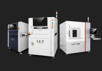
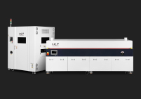
Choosing between 2D and 3D AOI depends on the complexity of the inspection task and budget requirements. Manufacturers in electronics often select 2D AOI or an SMT AOI Testing Machine for simpler, cost-sensitive applications, where speed and reliability matter most. However, 3D AOI or automatic optical inspection becomes essential for high-density, complex boards that demand superior defect detection and reliability. Automated optical inspection should match the specific needs of the production line. When comparing 2D vs 3D AOI, decision-makers must evaluate board complexity, reliability expectations, and available resources.
· 2D AOI uses flat images from a single angle, making it fast and cost-effective for simple, high-volume PCB inspections.
· 3D AOI captures detailed 3D maps with multiple cameras, detecting hidden and complex defects that 2D AOI often misses.
· Choose 2D AOI for quick, surface-level defect detection on standard boards where speed and budget matter most.
· Opt for 3D AOI when inspecting complex, dense boards requiring precise height and volume measurements for high reliability.
· Hybrid AOI systems combine 2D and 3D methods to balance speed, cost, and accuracy for diverse inspection needs.
· Consider board complexity, reliability demands, and budget carefully to select the AOI system that fits your production goals.
· Investing in 3D AOI supports future-proofing by handling miniaturized components and reducing false defect calls.
· Proper training and system integration with factory software improve inspection accuracy and streamline production.
Aspect | 2D AOI Systems | 3D AOI Systems |
Speed | Faster; ideal for high-volume production | Slightly slower; recent advances have improved speed |
Cost | Lower; mature and cost-effective technology | Higher; advanced imaging increases investment |
Defect Detection | Surface-level defects only; higher false calls | Detects hidden, volumetric, and surface defects; up to 30% more defects found |
Limitations | No depth measurement; cannot inspect hidden joints | Higher cost; more complex setup and maintenance |
Advantages | High throughput; flexible; less shadowing issues | Accurate height/volume measurement; comprehensive inspection |
2D AOI captures flat images using a single camera, making it suitable for rapid inspection of standard PCBs. This method excels at identifying visible, surface-level defects such as missing wires or incorrect components. 3D AOI, on the other hand, uses multiple cameras and structured light to create detailed 3D maps. This approach enables accurate measurement of height, volume, and shape, allowing detection of complex defects that 2D systems might miss. While 2D AOI offers faster processing and lower cost, 3D AOI provides superior defect detection and reduces false positives, especially in complex manufacturing environments.
 |
Best Use Cases
Selecting the right automated optical inspection method depends on the complexity of the board, the required reliability, and the production environment.
· 2D AOI Best For:
o High-speed, high-volume manufacturing lines where cost and throughput matter most.
o Inspection of simple or standard PCBs with mostly surface-level components.
o Detection of visible defects such as missing components, polarity errors, and incorrect placements.
o Environments where rapid changeover and flexible inspection are priorities.
· 3D AOI Best For:
o Complex, densely populated PCBs that require precise measurement of solder joints and component height.
o Applications demanding high reliability, such as automotive, aerospace, or medical device manufacturing.
o Detection of hidden or volumetric defects, including lifted leads, insufficient solder, and tombstoning.
o Production lines where reducing false calls and improving defect detection rates are critical.
The 2d vs 3d aoi debate centers on balancing speed, cost, and inspection accuracy. 2d AOI systems remain the preferred choice for straightforward, high-volume applications. 3d AOI systems deliver unmatched performance for advanced defect detection in challenging environments. Automated optical inspection continues to evolve, offering manufacturers the flexibility to match their inspection strategy to the specific needs of their PCBs and production goals.
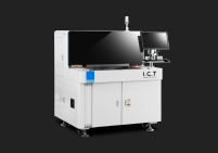
2D AOI uses high-resolution cameras to capture flat images of printed circuit boards during the inspection process. The system compares these images to reference data, identifying any differences that may indicate defects. Lighting plays a crucial role, as it highlights features and potential issues on the board’s surface. The technology relies on single-angle image capture, which means it inspects only what is visible from above. This approach allows for rapid inspection of large volumes of boards, making it ideal for high-speed manufacturing environments.
A key advantage of 2D AOI lies in its cost-effectiveness. The following table outlines typical costs associated with implementing 2D AOI in a standard SMT production line:
Cost Component | Typical Cost Range (USD) |
Basic to Mid-level 2D AOI | $3,200 to $20,000 |
Advanced 2D AOI Systems | $30,000 to $60,000 |
Example: YUSH YS-820L | $26,000 |
Installation Costs | $5,000 to $15,000 |
Software Licensing (annual) | $2,000 to $12,000 |
Training (per employee) | $1,000 to $5,000 |
This cost structure makes 2D AOI accessible for many manufacturers, especially those focused on high-volume production.
2D AOI delivers several strengths that benefit electronics manufacturing. The system inspects boards much faster than manual visual inspection. Manual methods suffer from human fatigue and inconsistency, but 2D AOI maintains high throughput and consistent results. The table below highlights the differences:
Feature | Manual Visual Inspection | 2D AOI Inspection |
Inspection Speed | Slower due to human fatigue and subjective judgment | Faster processing and analysis suitable for high-volume production |
Throughput | Limited by human speed and consistency | Significantly higher throughput enabling rapid inspections |
Consistency | Less consistent, prone to errors | High consistency without fatigue or subjectivity |
Manufacturers value 2D AOI for its ability to detect defects early in the process, preventing faulty boards from advancing and reducing costly rework. The system offers:
· High precision using advanced image processing.
· Fast inspection speeds for high throughput.
· Consistent, objective results.
· Reduced human error.
· Quick setup for different board designs.
· Classification of defects by type and severity.
· Data logging for quality control.
· Long-term cost savings.
· Continuous quality improvement.
· Seamless integration with SMT lines.
· Real-time feedback for immediate correction.
· Non-contact inspection to protect components.
Despite its advantages, 2D AOI has limitations. The system cannot perform true co-planarity inspection or provide volumetric measurement data. It often produces a higher false call rate compared to more advanced systems. Some common challenges include:
· Inability to inspect hidden solder joints or defects beneath components.
· Restricted height measurement, making it difficult to assess taller or irregularly shaped parts.
· Missed subtle or hidden solder defects, such as small voids.
· Increased false calls, requiring additional verification steps.
These limitations mean that 2D AOI works best for planar defects and simple boards. For complex assemblies or critical applications, manufacturers may need to supplement 2D AOI with other inspection methods.
2D AOI systems play a vital role in modern electronics manufacturing. Companies rely on 2d aoi to maintain high quality and efficiency on their production lines. The technology excels at inspecting printed circuit boards (PCBs) for surface-level defects. Manufacturers choose 2d aoi because it offers fast, reliable, and consistent inspection without slowing down production.
Electronics manufacturers use 2d aoi most frequently. The system checks for missing components, incorrect placements, and soldering errors. High-resolution cameras and advanced image processing allow 2d aoi to detect even small defects quickly. This capability supports high-volume production, where speed and accuracy are essential.
Tip: 2D AOI is ideal for manufacturers who need to inspect large numbers of simple or standard PCBs every day.
The following list highlights common applications of 2d aoi in the electronics industry:
· Surface-Mount Technology (SMT) Assembly: 2d aoi inspects boards after component placement and soldering. It identifies misplaced, missing, or skewed components.
· Through-Hole Technology (THT) Inspection: The system checks for correct insertion and soldering of through-hole parts.
· Solder Paste Inspection: 2d aoi verifies the presence and alignment of solder paste before reflow soldering.
· Final Assembly Verification: The technology ensures that all components are present and correctly oriented before the product moves to the next stage.
· Quality Control Audits: Manufacturers use 2d aoi for random sampling and audits to maintain process control.
2d aoi also finds use in other industries that require fast, surface-level inspection. However, electronics manufacturing remains the primary field due to the need for rapid, high-volume PCB inspection. Automotive and medical device industries often require more advanced inspection, so they tend to use 3D AOI for complex boards with hidden joints.
A typical 2d aoi workflow involves the following steps:
1. The system captures a flat image of the PCB using a high-resolution camera.
2. Image processing software compares the captured image to a reference.
3. The system flags any differences as potential defects.
4. Operators review flagged boards for further action.
2d aoi provides a cost-effective solution for detecting defects early in the process. By catching errors before final assembly, manufacturers reduce rework and scrap. The technology supports continuous improvement and helps companies meet strict quality standards.

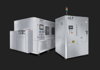
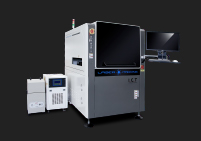
3D AOI systems use advanced imaging techniques to capture detailed information about printed circuit boards. These systems employ multiple cameras and structured light, such as Moiré technology, to scan the board from several angles. Koh Young’s 3D AOI, for example, uses proprietary multi-projection Moiré technology to generate true volumetric data. This approach measures height, volume, and coplanarity of solder joints and components. High-resolution cameras, sometimes with 8µm or 15µm resolution, allow precise measurement of even the smallest parts. The Z-axis extension increases the height measurement range, making it possible to inspect tall components. Specialized algorithms process the 3D data, measuring pin height, solder fillet height, and detecting bridges. The system performs imaging and inspection in parallel, which enables fast and accurate 3D measurements. This depth-based imaging significantly improves defect detection accuracy by reducing false calls and escapes.

3D AOI offers several advantages for electronics manufacturing, especially when inspecting complex or densely populated PCBs. The technology provides high accuracy and precision in defect detection. It captures detailed topographical data, allowing inspection of height variations and surface features that are critical in complex assemblies. 3D AOI detects three-dimensional defects such as warping, bending, and lifted leads—issues that 2D AOI often misses. The system inspects not only the top surface but also the sides and bottom of components, enabling detection of defects like tombstoning and skewed parts. Advanced software algorithms, including machine learning, enhance defect detection accuracy and adaptability. 3D AOI systems deliver faster inspection speeds than manual methods and do not require physical contact, preserving delicate components. The adaptability of 3D AOI suits industries with evolving PCB complexity, such as automotive, aerospace, and medical devices. Compared to Automated X-ray Inspection, 3D AOI remains more cost-effective for surface inspection while still providing detailed analysis.
Tip: 3D AOI excels at identifying three-dimensional defects that impact reliability in high-density and high-reliability applications.
Despite its strengths, 3D AOI has some limitations. The systems are more complex and expensive than 2D AOI, resulting in higher initial investment and maintenance costs. 3D AOI requires greater computational power to process the large volumes of 3D data, which can slow down inspection speed. Scanning methods, such as laser triangulation, involve detailed surface scanning and may reduce throughput compared to 2D AOI. These factors make 3D AOI less suitable for simple, high-speed production lines where cost and speed are the main priorities. Manufacturers must weigh these limitations against the need for advanced defect detection and comprehensive inspection.
3D AOI systems have become essential tools in modern electronics manufacturing. Their advanced imaging capabilities allow manufacturers to inspect complex assemblies with high accuracy. These systems use depth perception and multiple viewing angles to detect defects that traditional 2D methods often miss.
Many industries rely on 3d aoi for their most demanding inspection tasks. The technology supports high-speed production lines, where thousands of parts move through inspection every hour. Operators receive immediate feedback, which helps them adjust processes and maintain quality standards.
Note: 3D AOI maintains inspection speed without sacrificing accuracy, making it ideal for high-throughput environments.
Manufacturers choose 3d aoi for several critical applications:
· High-density SMT and SMD assembly lines, where miniaturized and densely packed components require precise inspection.
· Detection of defects such as improper polarity, misalignment, and missing parts, which are difficult to identify with 2D systems.
· Measurement of solder joint volume and shape, overcoming issues like specular reflections and shadowing that limit 2D AOI.
· Compensation for board warpage and inter-reflection, which can cause inaccuracies in 2D inspections.
· Inspection of complex boards in industries with strict quality requirements, including consumer electronics, automotive, and aerospace sectors.
3d aoi systems excel in environments where reliability cannot be compromised. Automotive and aerospace manufacturers, for example, depend on 3d inspection to catch hidden defects that could lead to product failures. Consumer electronics companies use 3d aoi to ensure that every device meets high performance and safety standards.
A typical 3d aoi workflow involves scanning the board from multiple angles. The system creates a detailed 3d map, measuring the height and volume of each component and solder joint. Advanced algorithms analyze this data, flagging any deviations from the standard. Operators can then review flagged items and take corrective action.
The flexibility of 3d aoi allows it to adapt to new board designs and evolving manufacturing requirements. As electronic components become smaller and more complex, 3d inspection ensures that quality remains consistent. Manufacturers benefit from reduced false calls, improved defect detection, and optimized production processes.
Tip: 3D AOI is the preferred choice for manufacturers who need precise, reliable inspection in fast-paced, complex production environments.
Detection capabilities set the foundation for any automated optical inspection system. In the 2d vs 3d aoi comparison, each method offers unique strengths and weaknesses. 2d aoi systems rely on top-down imaging to identify surface-level defects. These systems excel at spotting missing components, polarity errors, and solder paste misapplication. However, they struggle with hidden or volumetric defects because they lack depth perception.
3d aoi systems use structured light and multiple cameras to create a three-dimensional map of the board. This approach allows for precise measurement of component height, coplanarity, and solder volume. As a result, 3d aoi detects issues like lifted pins, insufficient solder, and package warpage—defects that 2d aoi often misses.
The following table highlights the differences in false positive rates and defect detection accuracy:
AOI System Type | False Positive Rate | Defect Detection Accuracy | Notes on False Negatives |
Legacy 2D AOI (rule-based) | Up to ~50% | ~85–90% | Higher due to lack of depth info |
AI-enhanced 3D AOI | Reduced to under 10% (4–6%) | 97–99% | Lower due to 3D depth data |
3d aoi systems significantly reduce false positives and improve overall defect detection. Manufacturers who require advanced inspection capabilities often choose 3d aoi for its superior performance.
Note: 3d aoi provides a more comprehensive inspection by capturing both surface and volumetric defects, making it ideal for complex assemblies.
Speed and cost play a critical role in selecting an aoi system. 2d vs 3d aoi systems differ greatly in these areas. 2d aoi offers faster inspection speeds and lower initial investment. These systems require less complex setup and minimal operator training. Manufacturers can deploy 2d aoi quickly in high-volume environments.
3d aoi systems demand a higher initial purchase price and more specialized setup. The technology requires calibration, ongoing training, and greater computational power. Maintenance costs also tend to be higher due to system complexity. However, 3d aoi delivers improved inspection capabilities and can reduce costly defects over time.
The table below compares the total cost of ownership and operational demands:
Aspect | 2D AOI Systems | 3D AOI Systems |
Initial Purchase Price | Starts around $3,200 | Can exceed $110,000 |
Annual Maintenance Cost | $5,000 to $15,000 (lower end) | $5,000 to $15,000 (higher end) |
Standard setup | Specialized setup, calibration, and training | |
Operational Demands | Lower complexity | Higher complexity, specialized knowledge |
ROI Consideration | Lower upfront and maintenance costs | Higher costs, but improved defect detection |
3d aoi systems require a larger investment but offer long-term benefits through enhanced defect detection and reduced rework. Smaller manufacturers may prefer 2d aoi for its affordability and ease of use.
Application suitability depends on the type of printed circuit board assembly and the required inspection capabilities. 2d vs 3d aoi systems each serve different production needs. 2d aoi works best for simpler PCB assemblies with mostly surface-level features. These systems provide fast, cost-effective inspection for standard boards and early stages of the SMT line.
3d aoi excels in inspecting complex assemblies that require depth measurement and coplanarity checks. The technology identifies defects involving component height, solder volume, and warpage. Industries such as automotive, aerospace, and medical devices often rely on 3d aoi to meet strict quality standards.
The table below summarizes which AOI type fits each application:
AOI Type | Suitable PCB Assembly Types | Key Inspection Capabilities | Reasoning |
2D AOI | Simpler PCB assemblies with less complex 3D features | Surface-level defects such as solder paste misapplication, polarity errors, missing parts | Cost-effective and fast; deployed early in SMT line; limited to top-down imaging |
3D AOI | More complex PCB assemblies requiring depth measurement and coplanarity checks | Defects involving component height, volume, coplanarity such as insufficient solder, lifted pins, package warpage | Uses structured light and multi-angle cameras for precise 3D defect detection |
Tip: Manufacturers should match their automated optical inspection system to the complexity of their boards and the reliability requirements of their industry.
The 2d vs 3d aoi decision shapes the effectiveness of inspection and the overall quality of finished products. By understanding the strengths of each system, manufacturers can optimize their inspection process and achieve better results.
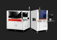
Hybrid AOI systems bring together the best features of both 2D and 3D inspection technologies. Manufacturers use these systems to address the growing complexity of modern printed circuit boards. By combining two inspection methods in one machine, hybrid AOI systems deliver flexible, efficient, and comprehensive quality control.
Hybrid AOI systems offer several key advantages:
· 2D AOI provides reliable, high-quality imaging for visible components. It works well for detecting simple defects and keeps inspection costs low.
· 3D AOI extends inspection capabilities to hidden solder joints, height measurements, and complex defect detection. It finds issues that 2D AOI cannot see.
· Hybrid systems apply 2D AOI where it is sufficient and switch to 3D AOI for advanced inspection. This approach saves time and money while improving defect coverage.
· Manufacturers can inspect products quickly and efficiently, matching the inspection method to the specific needs of each board area.
Yamaha Motor’s YRi-V hybrid AOI system demonstrates how this technology works in practice. The YRi-V integrates 2D and 3D inspection with a 4-direction angular camera and an 8-direction 3D projector. This setup achieves industry-leading inspection speed and precision. The system excels at inspecting ultra-small, fine-pitch components and mirror-surface finishes, which are difficult for traditional AOI systems. AI-powered automation in the YRi-V simplifies inspection data creation and tuning. Operators need less specialized skill, making the system easier to use. The hybrid approach supports fast, precise inspection of diverse and complex PCB components. It meets the demands of modern SMT production, where boards are smaller, denser, and more functional than ever before.
Tip: Hybrid AOI systems help manufacturers balance speed, cost, and inspection accuracy. They provide a practical solution for the 2d vs 3d aoi challenge in today’s electronics industry.
Hybrid AOI systems continue to evolve. As PCBs become more complex, these systems will play a bigger role in ensuring product quality and reliability. Manufacturers who invest in hybrid AOI gain the flexibility to adapt their inspection strategy as technology advances.

Board complexity plays a central role in selecting the right AOI system for any printed circuit board assembly. As the number of components, density, and use of advanced package technologies increase, manufacturers need inspection data that is both reliable and repeatable. Simple boards with mostly surface-level components benefit from 2D AOI. These systems use top-down imaging to check for missing parts and soldering errors. They offer fast inspection and cost savings, making them ideal for high-volume PCB production.
However, as complexity rises, 2D AOI faces challenges. Shadows, lighting variations, and the lack of depth information limit its effectiveness. Complex PCBs often feature miniaturized components, dense layouts, and multilayer designs. In these cases, 3D AOI becomes essential. 3D AOI systems use multiple cameras or laser technology to capture height and volume data. This allows them to detect defects like warping, lifted leads, and coplanarity issues—problems that 2D AOI cannot see.
Manufacturers in industries such as automotive and industrial electronics rely on 3D AOI for complex boards. These systems provide comprehensive measurement data that meets IPC-610 standards. This enables early detection of process drift and supports zero-defect goals.
AOI System | Minimum Board Complexity Typically Handled | Maximum Board Complexity Typically Handled |
2D AOI | Simpler boards with surface-level inspections; effective for detecting missing components and soldering errors; prioritizes speed and cost-effectiveness | Less complex boards without volumetric or height-related defects; generally not suited for multilayer or high-density boards |
3D AOI | Boards requiring volumetric inspection including height measurement; suitable for detecting complex defects like lifted leads and coplanarity issues | High-density, multilayer, and complex board layouts demanding detailed 3D defect detection; used in automotive and industrial electronics sectors |
Tip: For high-density, multilayer, or miniaturized PCBs, 3D AOI provides the measurement accuracy and defect detection needed for reliable inspection.
Reliability requirements differ across industries and directly influence AOI selection. Sectors such as automotive, aerospace, and medical devices demand the highest levels of product reliability. In these fields, even a single defect can lead to costly recalls or safety issues. AOI systems must deliver consistent, accurate inspection results to meet strict quality standards.
Several factors shape reliability in AOI selection:
Factor | Explanation |
Type of inspection | Determines if the AOI inspects at the board, component, or SMT level, matching industry needs. |
Image resolution | High resolution is critical for detecting tiny defects common in high-reliability sectors. |
Speed of inspection | Must match production scale; high throughput is needed without missing defects. |
Automation features | Automation reduces human error, supporting consistent quality in critical industries. |
Accuracy and reliability | Fundamental for meeting stringent standards and ensuring defect detection consistency. |
Integration with other systems | Seamless integration supports complex production lines typical in automotive/aerospace. |
After-sales support | Ongoing support ensures long-term reliability in demanding sectors. |
AOI systems enable early fault detection, which reduces costly production errors and improves the reliability of electronic devices. Advanced AOI technologies, including AI and 3D imaging, adapt to complex PCB designs and lower defect rates. For example, AOI equipment can reduce defect rates from 2% to 0.5% by automating inspections that would otherwise be manual and time-consuming. This improvement in defect detection leads to higher product reliability and customer satisfaction.
Note: Selecting the right AOI system for high-reliability industries ensures that every printed circuit board assembly meets the strictest quality standards.
Budget remains a key consideration when choosing between 2D and 3D AOI systems. 2D AOI offers a lower initial investment and reduced maintenance costs. These systems suit manufacturers focused on high-volume, cost-sensitive PCB production. They provide fast inspection for simpler boards, helping companies control expenses.
3D AOI systems require a higher upfront investment. The advanced imaging technology and software features add to the cost. Maintenance and operator training also increase expenses. However, 3D AOI delivers long-term value by reducing defect rates and improving product reliability. For complex PCBs, the investment in 3D AOI often pays off through fewer failures and less rework.
Manufacturers should weigh the total cost of ownership against the benefits of improved inspection accuracy. Selecting AOI equipment based on production volume, product complexity, and reliability goals ensures the system meets both budget and quality requirements. Proper training and regular maintenance help maximize the return on investment.
Tip: For manufacturers with limited budgets and simple boards, 2D AOI offers a practical solution. For those producing complex electronics or requiring high reliability, investing in 3D AOI can lead to significant long-term savings.
Selecting an AOI system is not just about meeting today’s inspection needs. Manufacturers must also consider how their investment will perform as technology and industry requirements evolve. The electronics industry continues to move toward greater miniaturization, higher component density, and stricter quality standards. These trends push AOI systems to deliver more accurate, reliable, and data-rich inspections.
2D AOI systems rely on image comparison and contrast. This approach works well for simple boards but struggles with complex or miniaturized components. As a result, 2D AOI often produces higher false call and escape rates. Quasi-3D or 2.5D systems offer some improvements but still face similar limitations. In contrast, true 3D AOI systems use measurement-based inspection. They provide accurate data on component height, solder joint volume, and coplanarity. This reduces false calls and escapes, helping manufacturers optimize processes and move closer to zero-defect production. For companies aiming for high-quality manufacturing, investing in 3D AOI often makes sense, even with higher upfront costs.
The table below summarizes key factors that influence future-proof AOI decisions:
Aspect | Summary |
Drivers | Miniaturization, complex electronics, demand for zero-defect products, growth in automotive/medical sectors |
Challenges | High initial cost and complexity of 3D AOI, need for specialized programming, ongoing updates |
Opportunities | AI/ML integration for better defect detection, expansion into advanced packaging, user-friendly interfaces |
Future Trends | Shift to true 3D AOI, AI/ML for predictive analytics, real-time inline inspection, digital MES/ERP integration, sustainability focus |
Regional Market Trends | Asia-Pacific leads in volume; North America/Europe focus on high-value, high-reliability sectors |
Investment Justification | 3D AOI reduces false calls, provides reliable data, supports Industry 4.0, essential for premium manufacturing |
Tip: Manufacturers planning for the future should look for AOI systems that support AI and machine learning, real-time data integration, and compatibility with digital manufacturing systems.
As AOI technology advances, systems with flexible software, modular hardware, and strong vendor support will adapt more easily to new requirements. Companies should also consider the ease of software updates, the ability to handle new component types, and the system’s integration with factory data networks. Choosing a future-ready AOI system helps manufacturers stay competitive as industry standards and customer expectations rise.
Manufacturers should select 2D AOI for efficient, cost-effective inspection of simple pcba assemblies, while 3D AOI suits complex boards with strict quality demands. Aligning AOI technology with inspection needs, product complexity, and budget ensures optimal results. Companies benefit from consulting AOI vendors, conducting trials, and reviewing system calibration and support before finalizing decisions. Revisiting the comparison and decision guide helps ensure the chosen solution matches evolving production requirements.
2D AOI inspects boards using flat images from a single angle. 3D AOI uses multiple angles and structured light to measure height and volume, detecting more complex defects.
2D AOI cannot detect hidden solder joint problems. It only inspects visible surfaces. 3D AOI provides depth information and can identify hidden or volumetric defects.
2D AOI works best for high-speed, high-volume production. It offers faster inspection and lower costs. 3D AOI suits slower lines with complex boards.
3D AOI systems need more maintenance and calibration. Their advanced cameras and software require regular updates. 2D AOI systems have simpler upkeep.
AOI systems catch defects early in the process. They prevent faulty boards from moving forward. This reduces rework, lowers costs, and improves overall product reliability.
Hybrid AOI systems combine the strengths of both 2D and 3D inspection. They offer flexible, comprehensive coverage. Manufacturers with varied board complexity often see strong returns from hybrid systems.
Operators need basic training for 2D AOI. 3D AOI and hybrid systems require more advanced skills, including calibration and software use. Many vendors provide training programs.
Most modernAOI systems support integration with MES or ERP software. This allows real-time data sharing and process control, supporting Industry 4.0 initiatives.