English


In the world of power electronics, ensuring reliability and efficiency is paramount. As devices become more compact and powerful, the challenges of reflow soldering in power electronics PCBA (Printed Circuit Board Assembly) grow exponentially. High-power components generate significant heat, demanding precise thermal management during the soldering process. Combine that with the complexity of managing PCB warpage, achieving consistent solder joint quality, and dealing with mixed-materials challenges, and you quickly realize that reflow soldering for power electronics is not your typical assembly task.
For manufacturers in this field, overcoming these hurdles is not just about optimizing the reflow profile – it's about pushing the boundaries of technology and finding innovative solutions that guarantee both performance and reliability. This article delves into the unique challenges faced during the reflow soldering of power electronics PCBA, offering insights into effective solutions, process enhancements, and future trends. From advanced reflow techniques to automation and real-time process monitoring, we will explore how the right strategies can turn these challenges into opportunities for higher yield, better quality, and greater product stability.
Let’s dive into the key challenges, the latest solutions, and the critical steps manufacturers must take to stay ahead in this ever-evolving industry.
In power electronics, managing heat efficiently during the reflow soldering process is not just a challenge — it’s a necessity. High-power components, such as power transistors, diodes, and inductors, generate substantial amounts of heat that must be carefully controlled throughout the assembly process. Failure to manage heat properly can lead to significant defects in solder joints, reduced performance, and even permanent damage to critical components. Let’s explore the two primary thermal management issues that arise when dealing with high-power components in power electronics PCBA.
One of the most pressing challenges in reflow soldering for power electronics is the high thermal mass of certain components. These components—often larger and more robust due to their power-handling capabilities—require more time and energy to heat up compared to smaller, less power-demanding components. This can create uneven heating across the PCB, resulting in areas where soldering doesn’t reach the required temperature for proper bonding.
For customers, this means increased risk of cold solder joints, which can lead to weak connections and, ultimately, higher failure rates in the field. Inconsistent heating can also affect the uniformity of the solder paste, leading to insufficient wetting of pads, poor solder joint formation, and issues with solderability. The key is to optimize the reflow profile to ensure all components reach their ideal soldering temperatures simultaneously, preventing underheating or overheating that can damage sensitive parts.
In practice, this might involve adjustments in the preheat and soak stages of the reflow process to ensure even heat distribution, particularly in areas with high thermal mass. It’s critical to strike a balance where the system allows larger components to gradually heat without causing excessive thermal gradients that can lead to defects.
Thermal shock is another serious concern when working with high-power components in power electronics. As components heat up, they expand, and as they cool down, they contract. If these thermal changes occur too quickly — especially during the cooling phase of the reflow soldering process — the component’s materials may not have enough time to adjust, leading to potential damage.
The risk of thermal shock is especially high when there is a sharp temperature transition between the reflow oven and the cooling section. For high-power components with large thermal mass, this rapid cooling can result in cracking, delamination, or even total failure of the component. When thermal shock occurs, the solder joints may also be compromised, which can lead to increased resistance, poor electrical performance, or complete system failure.
For customers, the practical consequences are clear: component damage caused by thermal shock leads to higher defect rates, more rework on the production line, and increased costs due to component replacements. Additionally, damaged components can degrade the long-term reliability of the product, affecting both warranty claims and customer satisfaction.
Mitigating thermal shock requires careful control of the cooling rate in the reflow oven. By adjusting the cooling phase to slow down the temperature drop, it allows components to cool at a more controlled rate, reducing stress and preventing damage. Ensuring a uniform and gradual transition from high to lower temperatures is key to maintaining the integrity of the components.
When it comes to power electronics PCBA, mechanical stability is a critical factor that directly impacts the quality and reliability of the final product. Among the various structural challenges, PCB warpage stands out as one of the most common and problematic issues in the reflow soldering process. Warpage refers to the bending or deformation of the PCB during the manufacturing process, which can severely affect the alignment of components, the integrity of solder joints, and overall assembly performance.
PCB warpage in power electronics is typically caused by a combination of factors, including the materials used in the PCB, the manufacturing processes, and the thermal stresses during reflow soldering. Let’s break down the primary causes:
Thermal Expansion and Contraction: The most significant contributor to PCB warpage is the uneven thermal expansion during the heating and cooling phases of the reflow process. High-power components, such as large capacitors, inductors, and heat-sensitive diodes, can create significant temperature gradients across the board. These differences in temperature cause different sections of the PCB to expand and contract at different rates, leading to bending or twisting.
Material Properties: The type of laminate material used in the PCB can also influence warpage. For example, certain PCB materials (such as FR4) have varying coefficients of thermal expansion (CTE) depending on their composition and layer structure. This can exacerbate warpage issues, especially in multi-layer PCBs where different layers expand at different rates.
Component Density and Placement: Power electronics PCBA often features high component density, which, while efficient for space utilization, can add to the warpage problem. Heavier components, especially large heat sinks or thick copper traces, can put additional mechanical stress on the PCB during the reflow process, contributing to deformation.
Improper Board Handling: During manufacturing and assembly, improper handling of the PCBs, such as excessive bending during transportation or mounting, can introduce stress that causes warpage before the reflow soldering even begins.
PCB warpage poses serious risks to both solder joint reliability and component alignment, which are crucial for the performance and longevity of power electronics products. Here’s how warpage impacts these factors:
Solder Joint Reliability: Warped PCBs can lead to misaligned solder joints, where the solder paste fails to bond correctly to the pads. This misalignment can cause issues like cold solder joints, voiding, or insufficient wetting, all of which compromise the strength and electrical conductivity of the solder joints. In power electronics, where high currents are often involved, this can lead to increased resistance and, in the worst case, failure of the solder joint under operational stress.
Component Alignment: When the PCB warps during reflow soldering, components may shift or tilt, leading to poor alignment on the board. This can result in tombstoning, where components become unstable and only one end is soldered, or bridging, where solder creates unwanted connections between adjacent pads. Both of these issues degrade the mechanical and electrical integrity of the assembly, affecting the product’s performance and reliability.
Increased Risk of Reliability Issues: Warped PCBs, particularly in high-power applications, can also lead to thermal cycling stress over time. As the components expand and contract during normal operation, the flexing of the PCB due to its warpage can cause solder joints to fatigue more quickly, potentially leading to premature failure in high-reliability applications like automotive, aerospace, or medical devices.
Impact on Automated Processes: Warpage also affects the precision of automated assembly processes like pick-and-place. Misalignment due to warpage can cause placement inaccuracies, leading to incorrect component positioning and the need for rework. This increases production time and costs, and can reduce throughput.
Soldering defects are a common challenge in power electronics PCBA, and they can have significant consequences on the performance and reliability of the final product. Power electronics assemblies often involve high-density components, complex thermal management requirements, and a variety of materials, which make them particularly susceptible to specific soldering defects. Understanding these defects and how to prevent them is essential for achieving high-quality solder joints and ensuring the longevity and reliability of power electronics products.
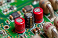
One of the most common soldering defects in power electronics PCBA is voiding, particularly in areas like thermal pads and BGA (Ball Grid Array) components. Voiding occurs when air or gases are trapped beneath the solder joint, leading to incomplete or weakened connections. In power electronics, where high currents are involved, even small voids can cause significant reliability issues, such as increased electrical resistance, overheating, and premature failure of the component.
The thermal pads in power electronics PCBA are typically used to dissipate heat generated by high-power components, and improper soldering can result in voids in these pads. This is particularly problematic as voids can interfere with the efficient heat dissipation needed to keep power components within operational temperature limits. For BGAs, which are commonly used in high-density power electronics assemblies, voiding beneath the solder balls can lead to weak connections and poor electrical conductivity. Voids in BGA joints can be challenging to detect using traditional visual inspection methods, making them a critical concern during reflow soldering.
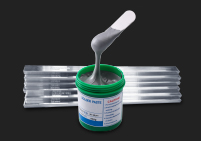
The wetting challenge is another related issue. Proper wetting occurs when the solder paste adequately adheres to the pads and the components, forming a strong and reliable bond. However, in power electronics, the combination of different materials (such as copper, aluminum, and gold) and large thermal masses can make it difficult for the solder to wet properly. If the solder fails to wet the pads or the BGA balls, it can result in poor joint quality, leading to weak mechanical bonds and reduced thermal and electrical conductivity.
Another common soldering defect in power electronics PCBA is tombstoning, which occurs when a component becomes tilted or stands upright, creating a poor solder joint. This defect often happens when the reflow temperature profile is not optimized, or when there is uneven heating across the PCB. In power electronics, where component alignment is crucial for performance, tombstoning can lead to weak connections that may fail under stress or thermal cycling. Additionally, tombstoning increases the risk of mechanical damage to components during assembly and operation.
Bridging is another issue that arises when excessive solder forms unwanted connections between adjacent pads. This typically happens when there is too much solder paste or when the reflow process causes the solder to spread excessively. In power electronics PCBA, where components are often placed close together, bridging can result in short circuits or signal interference, which could render the device inoperable. Ensuring the right amount of solder paste and optimizing the reflow profile are essential steps to avoid this defect.
Insufficient solder joints occur when the solder does not fill the joint completely, leading to weak or unreliable connections. This can result from an incorrect reflow profile, insufficient solder paste, or poor board cleaning before the soldering process. In power electronics, where high currents pass through solder joints, insufficient soldering can lead to high resistance connections, thermal hotspots, and eventual component failure. Ensuring consistent solder paste deposition and optimizing reflow parameters are key to avoiding this issue.
One of the most critical defects in power electronics PCBA is head-in-pillow, which occurs when the solder ball on a BGA component fails to fully wet to the pad, leaving a small void or gap between the solder and the pad. This defect is particularly problematic because it can be difficult to detect visually, yet it significantly compromises the reliability of the joint. Head-in-pillow defects can lead to poor electrical performance, increased resistance, and increased risk of failure under mechanical stress or thermal cycling. In power electronics, where reliability is paramount, detecting and preventing head-in-pillow defects is crucial for ensuring long-term performance.
Other reliability risks associated with soldering defects in power electronics PCBA include cold solder joints, poor mechanical adhesion, and delamination. Cold solder joints occur when the solder does not properly fuse with the component or pad, leading to weak connections. These types of defects are often caused by improper heating or cooling rates during the reflow process. Power electronics products, which operate under high loads, are particularly vulnerable to cold solder joints, as they can lead to increased resistance and overheating.
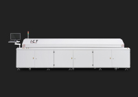
In power electronics PCBA, optimizing the reflow temperature profile is essential for ensuring high-quality solder joints and reliable component performance. The temperature profile directly affects the thermal behavior of both the PCB and its components during the reflow soldering process. Due to the high-power components used in these assemblies, which have unique thermal characteristics, the reflow profile must be carefully balanced to prevent defects such as warpage, insufficient solder joints, or thermal damage. In this chapter, we will explore how to balance the preheat, soak, reflow, and cooling stages to accommodate the demands of power electronics, particularly focusing on adjustments needed for lead-free solder and high-density designs.
A well-balanced temperature profile ensures that the entire PCB and all its components, particularly high-power ones, heat up and cool down at controlled rates. This helps to achieve uniform soldering, prevent thermal damage, and avoid warpage. Each stage of the reflow soldering process plays a crucial role in ensuring a successful assembly.
Preheat Stage: The preheat stage is critical for warming up the PCB and components before reaching the reflow zone. This gradual temperature increase helps prevent thermal shock to the components and avoids uneven heating that can cause warping. For high-power components, it's essential to ensure that the preheat temperature is high enough to allow the components to reach a uniform temperature, but not so high that it leads to thermal stress. Typically, the preheat temperature should be set between 150°C and 180°C, depending on the PCB material and component specifications.
Soak Stage: During the soak stage, the temperature is maintained at a constant level to allow the PCB and solder paste to stabilize. This stage is crucial for activating the flux in the solder paste and ensuring that the paste begins to melt uniformly. The soak temperature for power electronics PCBA should be carefully controlled to avoid overexposure to heat, which can cause components to overheat and suffer thermal damage. A typical soak temperature is 180°C to 200°C, but the duration should be adjusted based on the thermal mass of the components.
Reflow Stage: The reflow stage is where the solder paste melts and forms the solder joints. For power electronics, achieving uniform reflow across the board is vital. The temperature in this stage should typically reach between 220°C and 250°C for lead-free soldering, depending on the specific solder paste used. To avoid damaging high-power components, the reflow stage temperature should be controlled to prevent overheating, while ensuring that the solder paste reaches its reflow point for proper wetting and bonding.
Cooling Stage: Cooling is just as important as the heating process in maintaining the integrity of the solder joints and the PCB. Too fast a cooling rate can cause thermal shock, leading to component damage or PCB warpage. For power electronics, where components often have larger thermal masses, the cooling rate should be gradual and controlled. Cooling typically occurs in two phases: an initial rapid cooling phase followed by a slower, more controlled phase. This helps prevent thermal stresses and allows components to cool evenly, reducing the risk of cracks or other mechanical issues. Cooling rates of 2–4°C per second are generally recommended.
Balancing these stages is critical for optimizing the reflow soldering process. By carefully controlling the preheat, soak, reflow, and cooling temperatures, manufacturers can ensure that high-power components are heated and cooled evenly, avoiding thermal stresses that can affect both the component and solder joint integrity.
The shift to lead-free soldering and the increasing complexity of high-density designs in power electronics add additional challenges to reflow soldering, requiring specific adjustments to the temperature profile.
Lead-Free Soldering: With the transition to lead-free solder alloys, which generally have higher melting points than traditional tin-lead solder, the reflow temperature profile must be adjusted to accommodate these changes. Lead-free solder typically melts at temperatures between 217°C and 220°C, compared to around 183°C for lead-based solders. This means the reflow peak temperature needs to be raised to between 240°C and 250°C to ensure proper wetting and bonding. The increased temperature can put additional stress on high-power components, so it is essential to control the soak time and cooling rates to avoid component damage while still achieving strong solder joints.
High-Density Designs: Power electronics PCBA designs often feature high-density component placements with components placed very close together. This can lead to issues with heat distribution, as heat may not be evenly distributed across the PCB. As a result, the reflow profile may need to be adjusted to ensure uniform heating throughout the board, particularly for the high-power components that require more heat to reach the reflow temperature. This may involve optimizing the soak time to ensure uniform activation of the flux in solder paste, especially in areas with high component density.
Additionally, components with larger thermal masses, such as power transistors, capacitors, and inductors, will require more time to heat up. In high-density designs, it may be necessary to modify the preheat and soak phases to ensure that these components are brought up to temperature gradually, preventing overheating and potential damage. In some cases, the use of multiple reflow passes may be necessary for especially dense assemblies.
Convection vs. Infrared Heating: With high-density designs, the choice of heating method (convection vs. infrared) can also affect the temperature profile. Convection ovens tend to provide more uniform heating, which is beneficial for high-density PCBs, while infrared ovens may be better suited for localized heating. Manufacturers should select the appropriate heating method to ensure uniform soldering of all components.
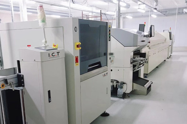
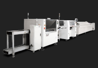
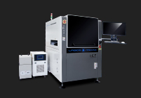
In the evolving landscape of power electronics manufacturing, achieving high-quality solder joints and ensuring production efficiency are paramount. Advanced reflow soldering techniques, along with automated inspection systems and real-time process monitoring, are essential for improving reliability, reducing defects, and optimizing overall manufacturing performance. This chapter explores how integrating nitrogen reflow soldering, SPI, AOI, and real-time process control can significantly enhance the reflow soldering process for power electronics.
Nitrogen reflow soldering has become a standard technique for improving solder joint quality in power electronics, where component reliability is critical. The use of nitrogen as a controlled atmosphere in the reflow oven has several advantages:
Reduced Oxidation and Improved Solder Wetting: Nitrogen helps to eliminate oxygen, reducing oxidation of the solder paste and component pads. This ensures better wetting and stronger, more reliable solder joints. For high-power components, which generate significant heat, reducing oxidation improves the mechanical and electrical reliability of solder joints.
Minimized Voiding: In power electronics, where components like BGAs and thermal pads are used, voids can be detrimental. Nitrogen reflow soldering significantly reduces void formation, ensuring complete solder joint formation and maintaining consistent electrical conductivity.
Enhanced Control Over the Process: Nitrogen reflow provides stable reflow conditions, helping to maintain consistent thermal profiles. This is especially important in power electronics, where variations in heat can lead to significant defects in high-density or high-power component areas.
Lead-Free Soldering Compatibility: As power electronics are increasingly using lead-free solder, nitrogen reflow soldering is particularly beneficial due to the higher melting points of lead-free alloys. The process maintains temperature control during the soak and reflow stages, reducing the risk of thermal damage to components.
The integration of SPI (Solder Paste Inspection), AOI (Automated Optical Inspection), and real-time process monitoring into the reflow soldering process has revolutionized quality control in power electronics PCBA. These systems work in tandem to catch defects early, prevent rework, and ensure that each assembly meets stringent quality standards.
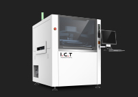
Solder Paste Inspection (SPI): SPI systems are used to inspect solder paste deposits immediately after the printing process. By using advanced 3D imaging, SPI detects issues like insufficient paste, misalignment, and excessive paste volume, ensuring that the paste is applied consistently and accurately. Early detection of these issues prevents defects like insufficient soldering or cold solder joints that may arise later in the reflow process. SPI also offers real-time feedback to adjust the printing process and maintain paste consistency.
Automated Optical Inspection (AOI): After the reflow process, AOI systems play a critical role in inspecting solder joints. These systems use high-resolution cameras to detect defects such as cold solder joints, bridging, misalignment, and tombstoning. For power electronics, where component reliability is key, AOI helps ensure that solder joints are uniform, strong, and electrically stable. The integration of AOI with the reflow soldering line allows for real-time defect detection and immediate corrective actions, which reduces the need for manual inspection and rework.
Real-Time Process Monitoring: Real-time monitoring tools provide live data on process parameters such as temperature profiles, conveyor speeds, and flux usage. By continuously tracking these factors during reflow soldering, manufacturers can quickly detect deviations from the ideal process conditions. If the temperature profile is off-target or if the conveyor speed is too fast or slow, adjustments can be made in real time to prevent defects. This real-time feedback ensures that each board is processed under optimal conditions, leading to improved yield and reduced waste.
Continuous Process Improvement: The data collected from SPI, AOI, and real-time monitoring systems can be analyzed to identify trends, detect recurring issues, and uncover areas for optimization. This data-driven approach supports continuous improvement by enabling manufacturers to make adjustments to the reflow soldering process based on real-time performance data. Over time, these improvements lead to a more efficient production process, higher yields, and reduced defect rates.
Process Integration and Automation: The integration of these systems into a fully automated production line enhances overall efficiency. Automation reduces the reliance on manual inspections, speeds up production, and minimizes human error. By integrating SPI and AOI directly with the reflow soldering equipment, manufacturers can achieve a more streamlined, automated process, which leads to higher throughput and lower operational costs.
One of the biggest challenges in power electronics PCBA is managing PCB warpage, especially in high-power inverter assemblies. Inverters, which convert DC to AC power, often contain large components with significant thermal masses. This makes the PCB more prone to warping during reflow soldering, which can lead to misalignment of components and poor solder joint formation.
In a recent case, a manufacturer of high-power inverters faced frequent warpage issues that led to tombstoning and insufficient soldering in key components, such as capacitors and inductors. To address this, the company optimized its reflow profile by adjusting the preheat and soak stages to allow for a more gradual temperature increase, reducing the risk of thermal shock. They also implemented support tooling during the soldering process to minimize the mechanical stress on the PCB.
The results were significant: after these changes, the manufacturer saw a 30% reduction in defects related to warpage and a marked improvement in solder joint reliability. The boards were able to handle thermal cycling without compromising performance, and yield rates improved significantly.
Another common challenge in power electronics is optimizing the reflow temperature profile to achieve consistent soldering results, particularly for high-density designs and lead-free soldering. In one case, a company manufacturing power supplies for industrial automation was facing inconsistent solder joints due to poorly optimized reflow profiles.
The company made several changes, including temperature profile optimization for the reflow oven, adjusting the soak time and cooling rate to match the needs of high-power components. Additionally, they integrated Automated Optical Inspection (AOI) at key points in the production process to catch defects early and adjust the reflow process in real-time.
These optimizations led to a 15% improvement in yield and a 25% reduction in rework time. The ability to immediately detect and correct defects using AOI helped the company significantly improve product reliability while reducing overall manufacturing costs.
As the demand for more efficient and environmentally-friendly electronics increases, manufacturers are turning to new materials and eco-friendly processes to improve the performance and sustainability of power electronics PCBA. One such trend is the development of low-temperature solder alloys, which not only reduce energy consumption during reflow soldering but also help minimize thermal stresses on sensitive components.
Additionally, lead-free soldering continues to be a priority, with advances in solder paste formulations that reduce toxicity and improve soldering consistency. Biodegradable flux and recyclable components are also gaining traction, contributing to a greener production process.
The use of advanced thermal management materials, such as graphene-based solder pastes and thermally conductive polymers, is another exciting development. These materials help power electronics dissipate heat more effectively, which is crucial for components that operate under high-power conditions. This trend aligns with the industry's growing focus on sustainability and reducing carbon footprints.
The integration of artificial intelligence (AI) into the reflow soldering process holds immense potential for improving efficiency and sustainability in power electronics manufacturing. AI-driven profiling allows for the real-time adjustment of reflow temperature profiles based on factors such as component size, thermal mass, and PCB layout, ensuring optimal soldering conditions for each unique board.
Furthermore, AI systems can predict potential defects before they occur by analyzing data from previous production runs and adjusting the reflow parameters accordingly. This not only improves solder joint quality but also reduces energy consumption by optimizing the reflow process and minimizing waste.
The application of AI also extends to predictive maintenance of reflow ovens, where AI can monitor equipment performance and predict when maintenance is needed before a breakdown occurs. This proactive approach reduces downtime and extends the life of manufacturing equipment, contributing to both cost savings and sustainability.
In conclusion, overcoming the challenges of reflow soldering in power electronics requires a combination of advanced techniques, process optimization, and the integration of cutting-edge technologies. From thermal management and warpage control to the use of nitrogen reflow soldering and inline inspection systems, each of these strategies plays a vital role in improving solder joint reliability, reducing defects, and enhancing overall production efficiency.
Key takeaways from this article include:
The importance of balancing reflow temperature profiles to manage thermal mass and prevent defects like warpage, voiding, and thermal shock.
The significant benefits of nitrogen reflow soldering for improving soldering quality and reducing oxidation and voiding.
The essential role of SPI and AOI in defect prevention and providing real-time feedback, ensuring high-quality power electronics assemblies.
The future trends in materials innovation and AI-driven profiling, which promise to further optimize the reflow soldering process and improve sustainability in electronics manufacturing.
As the power electronics industry continues to evolve, manufacturers must stay ahead by adopting the latest technologies and continuously improving their processes. By embracing advanced reflow soldering techniques and integrating automation, quality control, and real-time monitoring, they can ensure the production of reliable, high-performance power electronics assemblies.
What makes reflow soldering more challenging for power electronics PCBA compared to standard assemblies?
How can adjusting the temperature profile reduce voiding and warpage in power PCBA?
How does AOI help in detecting and preventing reflow defects in power electronics?
Is nitrogen reflow soldering worth the investment for high-reliability power PCBA?
How does I.C.T support manufacturers in overcoming these reflow challenges?