English
Views: 0 Author: Site Editor Publish Time: 2025-08-12 Origin: Site


PCBA inspection is critical in electronics manufacturing. It ensures product reliability and minimizes defects. Effective inspection methods like AOI, X-Ray, ICT, and Functional Testing help detect flaws early, preventing costly failures. In this post, you’ll learn how these testing methods work and why they’re essential for quality control.

PCBA inspection is the process of evaluating the quality of printed circuit board assemblies. It involves checking for defects like missing components, incorrect placement, or soldering errors. PCBA inspection is essential in electronics manufacturing to ensure that each board meets the required standards. It helps identify issues early, preventing costly failures down the line. Effective testing ensures product performance, reduces defects, and ensures the longevity of the final product. Without proper inspection, there’s a risk of products failing when they reach customers.
Modern PCBs are more complex than ever. Higher component densities, smaller packages, and new technologies make it harder to detect defects. Common defects include missing components, misalignments, or poor solder joints. As designs become more intricate, the opportunities for defects increase, which makes accurate inspection even more important. New package technologies like BGAs (Ball Grid Arrays) and CSPs (Chip Scale Packages) can hide defects beneath components, requiring advanced inspection techniques like X-ray inspection.
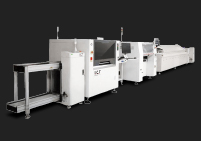
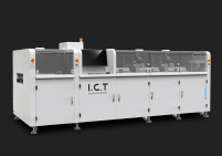
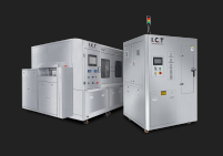
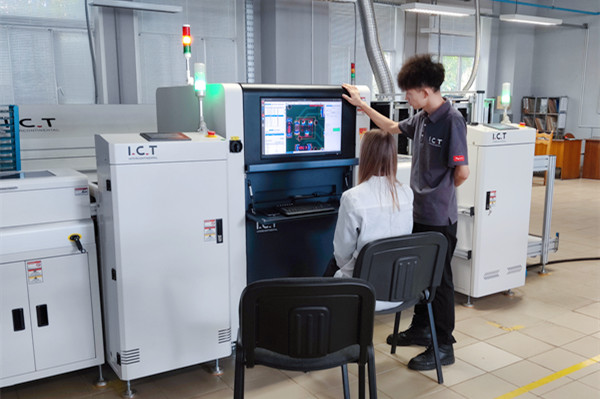
Automated Optical Inspection (AOI) is a non-invasive testing method used in PCBA to detect defects. It uses high-resolution cameras and specialized software to analyze PCBs for visual issues like missing components or misalignments. AOI systems work by capturing detailed images of the PCB’s surface. The software then compares these images to a reference design and flags any discrepancies. AOI has become crucial as PCBs grow more complex, with higher component densities and smaller packages.
Speed and Efficiency: AOI can scan boards quickly, identifying defects in a fraction of the time manual inspection would take.
Types of Defects AOI Can Detect:
Missing components.
Misaligned parts.
Soldering defects like bridges, cold solder joints, or insufficient solder.
Advantages Over Manual Inspection:
Reduces human error, ensuring consistent results.
Faster processing times allow for high-volume production.
To integrate AOI into the production process, follow these steps:
Pre-reflow Inspection: Place AOI before the soldering process to catch misplacements early.
Post-reflow Inspection: After soldering, AOI ensures that the solder joints are formed properly and that components are correctly placed.
Best Practices: Regularly update the software with new designs to keep up with PCB changes. Also, position AOI systems at key stages of production for maximum impact. AOI is especially effective in high-volume manufacturing, helping to detect defects before they propagate through later stages of production.
AOI is highly effective at surface inspection, but it cannot detect internal issues like hidden solder joints or electrical faults. For more comprehensive testing, combine AOI with methods like X-ray or ICT, which can look inside the board and check electrical functionality.
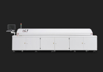
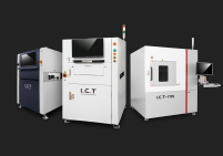
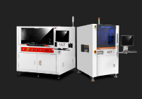
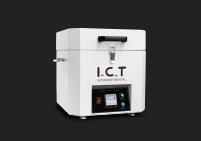
X-ray inspection uses radiation to generate detailed internal images of a PCB. Unlike AOI, which examines the surface, X-ray can detect hidden flaws, such as solder voids or cracks underneath components like BGAs (Ball Grid Arrays). It’s a deep inspection technique that helps identify issues invisible to traditional optical methods. X-ray inspection is especially useful for complex assemblies where traditional methods fall short.
X-ray inspection is vital for uncovering hidden defects that surface inspections can’t detect, such as:
Solder Voids: Gaps in solder joints that could lead to weak electrical connections.
BGA Issues: Problems beneath BGAs or CSPs (Chip Scale Packages), where solder joints are not visible. For complex PCBs with dense components, X-ray ensures reliability and durability, which is critical in industries like medical or automotive electronics where failure isn’t an option.
X-ray inspection works by passing radiation through the PCB to create images that reveal internal structures. It’s best used:
After soldering: To detect hidden issues like voids or improper solder joints.
When traditional methods fall short: Such as for components like BGAs or hidden solder joints. To ensure thorough inspection, integrate X-ray with other methods like AOI, which checks for surface defects, providing a comprehensive quality control process.
While X-ray provides in-depth insights, it has a few limitations:
Cost and Complexity: X-ray systems are expensive to acquire and maintain.
When Not Needed: It’s not ideal for surface-level issues, like misaligned components or visible soldering defects.
Cost-Effectiveness: The high detail X-ray offers may not justify the cost in simpler applications.
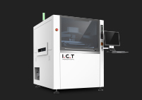
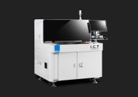
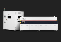
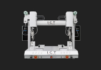
In-Circuit Testing (ICT) is a method used to test the electrical functionality of a PCB. It measures characteristics like voltage, resistance, and signal integrity to verify that each component is working as intended. ICT tests the electrical connections between components and ensures that the circuit behaves as designed. It can detect both manufacturing defects and design flaws, especially those related to electrical issues that might not be visible on the surface.
Comprehensive Electrical Testing: ICT can detect faults such as short circuits and open connections, ensuring the circuit functions correctly.
Identifying Defects Missed by AOI and X-ray: While AOI and X-ray focus on physical defects, ICT tests electrical performance, catching issues like signal integrity problems.
Full Circuit Testing: ICT checks the performance of the entire circuit, ensuring that all components are correctly functioning in relation to each other.
Set Up ICT Tests: ICT requires setting up test probes on specific test points across the PCB to measure electrical characteristics like voltage and current.
Timing in the Assembly Process: Perform ICT after component placement but before functional testing to catch any electrical issues early.
Best Practices: Optimize test point placement to ensure accessibility and minimize false negatives. Using the right test fixtures is key to accurate and reliable results.
Accessibility Issues: ICT requires clear access to test points, which can be difficult in densely packed PCBs.
Combination with Other Methods: ICT works best when combined with visual inspections like AOI or X-ray, as it cannot detect visual defects or soldering issues.
Not Ideal for Surface-Level Defects: It can't spot issues like component misplacement or poor soldering, which are better detected by AOI or X-ray inspection.
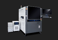
Functional testing verifies whether a PCBA works as intended in real-world conditions. Unlike AOI, X-ray, and ICT, which focus on detecting defects or electrical functionality, functional testing ensures the entire PCB operates correctly during use. It’s designed to detect performance-related issues that other methods can't catch, such as firmware errors or operational consistency problems.
Functional testing is critical for ensuring the final product performs its intended tasks. While AOI or ICT may detect physical or electrical defects, functional testing checks how the product operates in practice, like signal integrity or power distribution. For example, in the automotive industry, functional testing can identify issues in a PCB that would only be noticed during real-world use, such as power fluctuations or component behavior under stress.
Evaluate Performance: Test load capabilities, verify input/output functions, and check power and signal integrity.
Timing: Perform functional testing after assembly and once visual and electrical inspections (AOI, X-ray, ICT) are complete.
Best Practices: Include stress testing, ensure that all power routing and signal integrity are intact, and test specific functions like voltage levels or circuit responses.
Functional testing cannot identify manufacturing defects like poor soldering or component misplacement. It is best used in combination with other methods, like AOI or X-ray, for complete coverage. Additionally, it can be challenging to perform functional tests on very complex circuits or specialized assemblies, where custom testing setups may be needed.

When selecting a testing method, it’s important to compare the strengths and weaknesses of each one:
AOI: Best for detecting surface-level defects quickly, such as missing or misaligned components. It’s fast but limited to visual issues.
X-Ray: Essential for inspecting hidden defects like solder voids and issues under BGAs. It's detailed but more expensive and complex.
ICT: Focuses on verifying the electrical functionality of a PCB, detecting short circuits and resistance issues. It requires accessible test points.
Functional Testing: Tests the real-world performance of a board. It detects operational flaws that other methods miss, but it doesn’t identify physical defects. Factors to consider when choosing include:
Defect Type: What kind of issues do you need to detect? Electrical, mechanical, or functional?
Production Volume: AOI is great for high-volume production, while X-ray is better suited for critical, low-volume parts.
Cost: X-ray and ICT systems are more expensive than AOI, so balance budget and need.
Complexity of the PCB: More complex designs, such as those with BGAs or multilayer boards, often require X-ray or ICT. Tailor your testing strategy based on the industry needs—medical devices, automotive, and consumer electronics each have different requirements.
For a robust quality control process, combine multiple methods:
Pre-reflow AOI: Identify component misplacements and solder issues early.
X-Ray: Inspect hidden areas and defects in complex components like BGAs.
ICT: Ensure the board functions electrically, checking for shorts and open circuits.
Functional Testing: Test the PCB’s performance under real-world conditions, such as signal integrity and power distribution. Real-world examples show that combining these methods ensures comprehensive inspection. For example, in medical electronics, AOI and X-ray may be used for defect detection, followed by ICT to verify functionality. By integrating testing methods, manufacturers reduce the risk of defects and ensure product reliability.
Different industries adopt varying testing strategies:
Consumer Electronics: Often rely on AOI and ICT for fast, cost-effective testing, ensuring electrical functionality and surface-level defect detection.
Automotive: Require a more thorough testing approach, including X-ray and functional testing, to ensure long-term reliability and safety.
Medical Devices: Combine all four methods to meet the stringent safety and performance standards. Manufacturers decide the best mix of inspection methods based on product complexity, budget, and industry standards. Case studies show how combining AOI, X-ray, ICT, and functional testing leads to higher yields and fewer product failures.
Emerging technologies like AI, machine learning, and automated testing are revolutionizing PCB inspection. These innovations make inspections faster, more accurate, and more efficient by automating complex tasks.
AI and Machine Learning: AI is increasingly used to detect defects that were previously hard to identify. It learns from past inspections, improving accuracy over time. Machine learning models can now predict potential defects before they happen, reducing rework.
Automated Testing: More companies are adopting fully automated inspection systems that not only improve speed but also reduce human error. These systems can quickly adjust to changes in PCB designs and processes, ensuring consistency in high-volume production. These technologies are making PCB inspection more intelligent and streamlined, paving the way for faster product development cycles and better quality control.
As technology advances, so will the capabilities of traditional inspection methods:
AOI: The future of AOI lies in integrating AI-driven defect detection and 3D imaging, offering deeper analysis of complex PCBs.
X-Ray: X-ray inspection will continue to evolve, with advancements in 3D X-ray and micro-focus imaging providing more detailed and accurate internal views of PCBs, particularly for high-density boards.
ICT: In-circuit testing will become faster and more efficient as new testing fixtures and automated systems reduce setup time. Enhanced ICT will integrate more thoroughly with other inspection methods, providing a holistic view of the PCB's functionality.
Functional Testing: With growing complexity in PCBs, functional testing will integrate more real-time data analysis and sensor technology to better simulate real-world conditions and improve accuracy. Manufacturers can stay ahead of the curve by adopting these technologies early. Data analytics will also play a critical role in optimizing inspection processes, providing valuable insights into production efficiency and defect trends. These advancements will ensure that inspections are not just thorough but also predictive, allowing for preventive measures to be taken before defects occur.

Each inspection method—AOI, X-ray, ICT, and functional testing—plays a crucial role in ensuring a robust PCBA quality control process. By combining these methods, manufacturers can detect a wide range of defects, from surface-level issues to hidden electrical problems. Manufacturers should integrate multiple inspection techniques to optimize their PCBA testing process. This approach will reduce defects and improve overall product quality, ensuring higher reliability and customer satisfaction.
A1: AOI focuses on surface defects, while X-ray inspection is used to examine hidden solder joints and internal structures.
A2: ICT is ideal for verifying the electrical functionality of PCBs and detecting issues like short circuits or design flaws.
A3: No, functional testing is focused on verifying the functionality of the finished product, not detecting physical manufacturing defects.
A4: Choose based on the types of defects you need to detect, the complexity of the PCB, and your production needs.
A5: Yes, technologies like AI and machine learning are advancing inspection methods, making them faster and more accurate.