Views: 0 Author: Site Editor Publish Time: 2025-12-11 Origin: Site


In modern high-density SMT production, the most expensive mistakes are born in the solder paste printing stage—yet most factories only discover them hours later at AOI or functional test. If your line is already showing these five classic warning signs, you don’t just “need” SPI in SMT Line—you needed it yesterday.
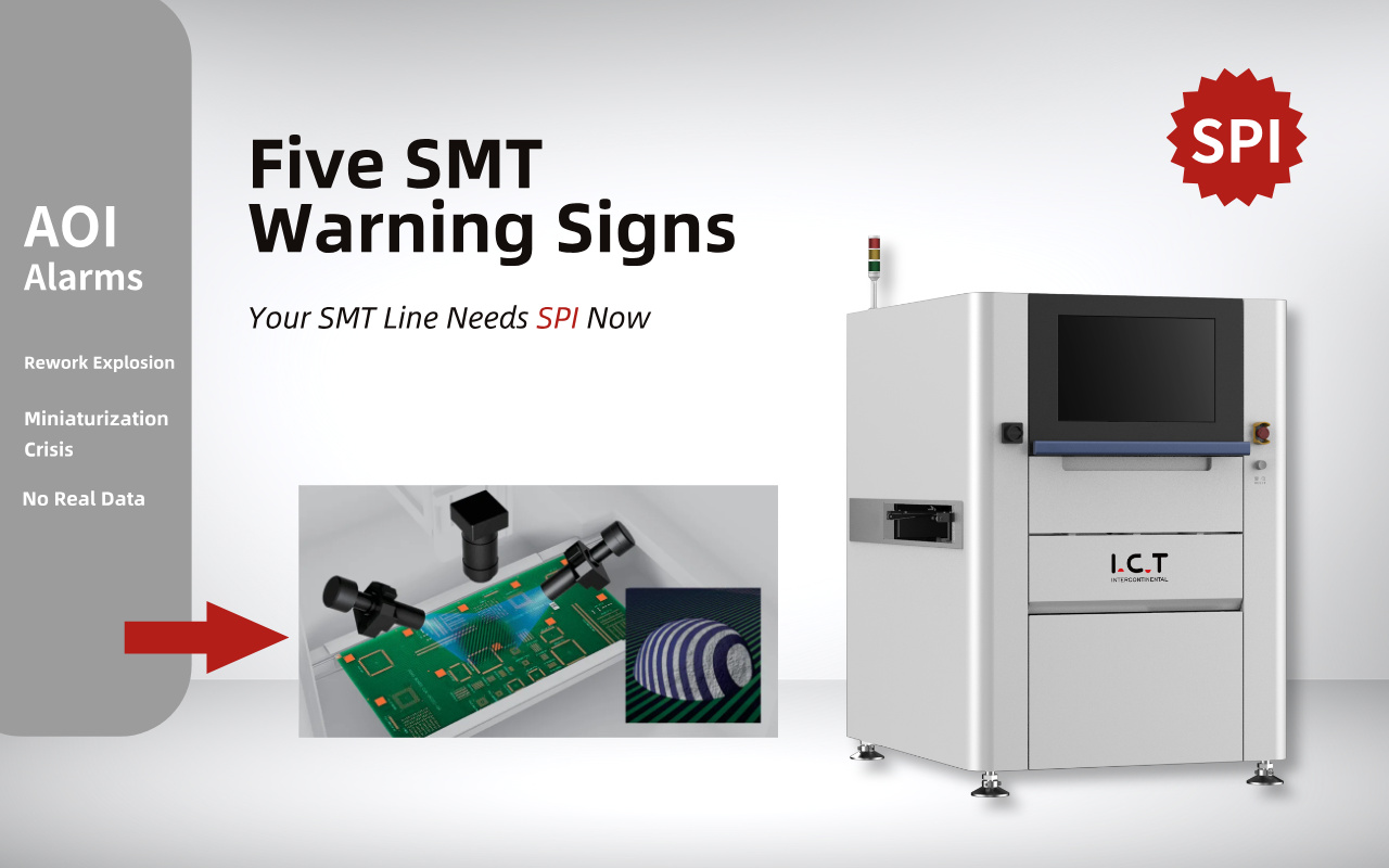
Imagine you walk to the AOI station every morning and see the same red error messages again and again: “insufficient solder,” “excessive solder,” or “bridging.” This is not bad luck—it is the first big warning sign that your solder paste printing step has a problem.
AOI is the machine that checks the boards after components are placed, so when it keeps finding solder paste issues, it means the trouble started much earlier, right at the printer. Most factories think AOI will catch everything, but by the time AOI sees the problem, the board has already gone through placement and maybe even reflow.
Fixing it now costs a lot of time and money. SPI, on the other hand, checks the solder paste immediately after printing, before any components are added. This way, bad boards never move forward, and you save hours of rework every day.
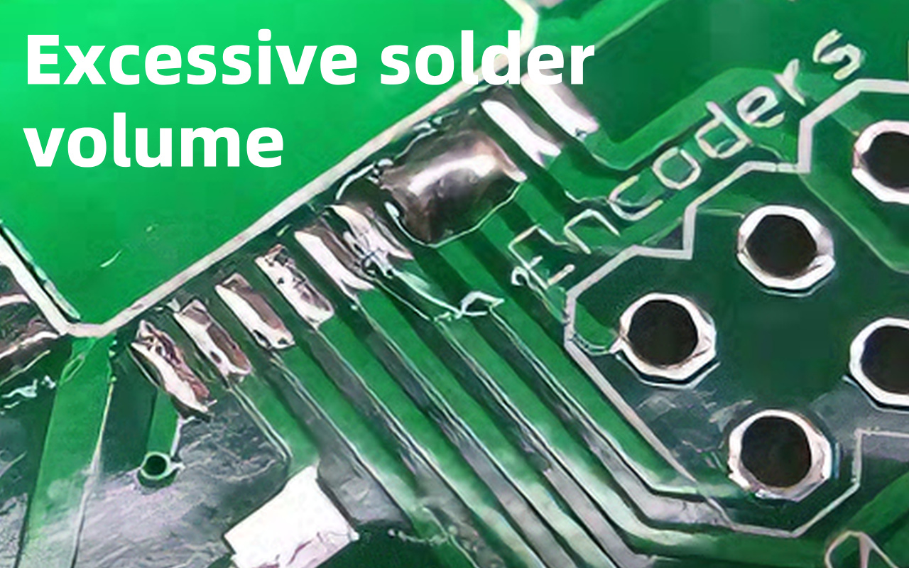
Insufficient solder means some pads have too little paste, so components may not connect properly after heating. Excessive solder means too much paste, which can cause shorts between nearby pads.
You might see one board with only 60% of the needed paste on a BGA ball, while the next board has 140% on the same spot. This happens because the printer is not putting down the same amount every time. Operators often blame the paste or the stencil, but the real reason is usually unstable pressure or speed.
Without measurement, you only discover it later at AOI. A simple SPI check right after printing would show the exact volume on every single pad and stop the problem immediately.
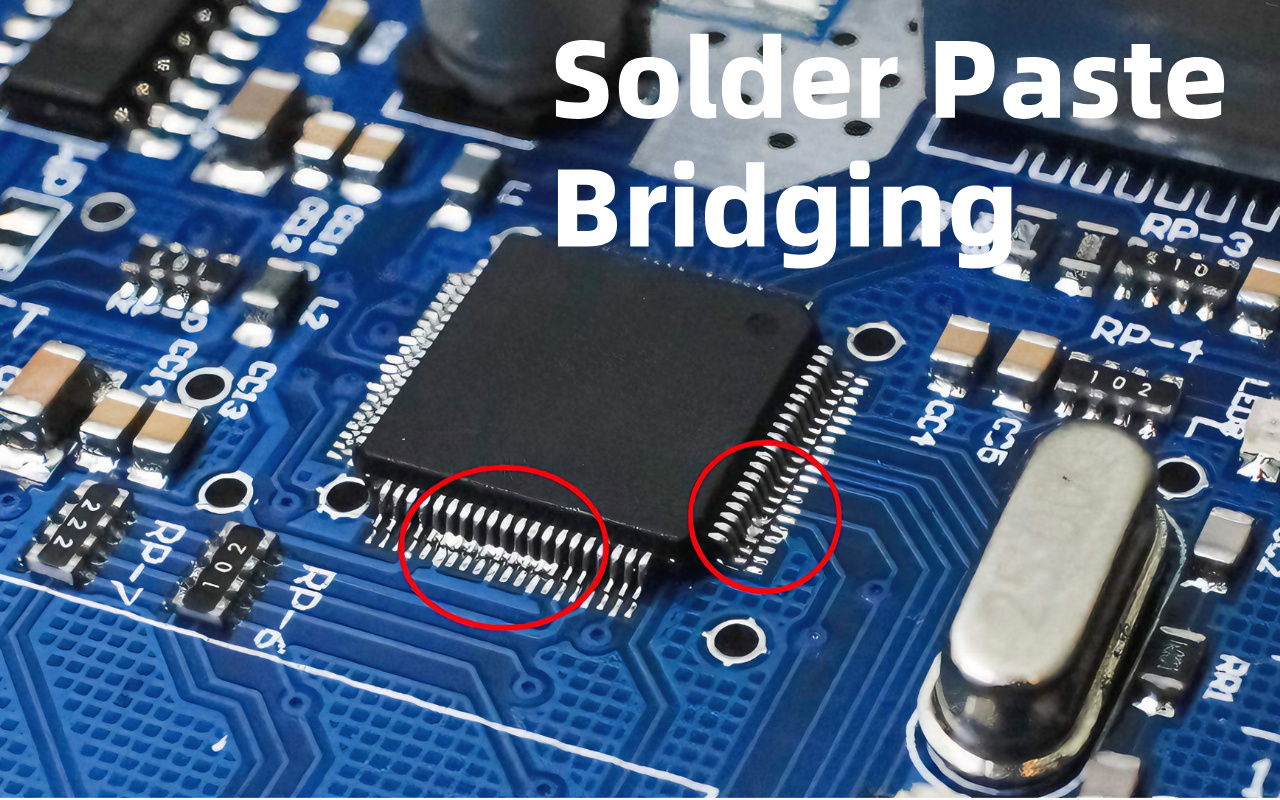
Paste offset means the solder paste is printed a little to the left or right of where it should be. Even a tiny shift of 25 microns (thinner than a hair) can make paste touch the next pad, creating a bridge. Bridging looks like little silver connections between pins that should be separate.
Engineers often say “the stencil is fine” or “placement caused this,” but most of the time the printer moved the paste during printing. Random bridging is especially common on fine-pitch parts like 0.5 mm or 0.4 mm components.
AOI will catch it, but the board is already full of expensive chips. SPI measures the exact position of every paste deposit in seconds, so you fix the printer before the next board even starts.
Every time AOI stops a board for a solder paste problem, your printer is sending you a message: “I need help!” Studies from IPC and SMTA show that 60% to 74% of all soldering defects start at the printing stage.
That means more than half of your rework time is caused by something that could be fixed in 10 seconds with SPI. Think of it like a car with a flat tire—you don’t wait until you crash to check the tires. Right now, AOI is telling you the tire is flat, but you are still driving.
Installing SPI is like adding a tire-pressure sensor: it warns you the moment pressure drops, so you never get a flat in the first place. Factories that add SPI usually cut paste-related defects by 70% in the first month.
If your engineers spend hours every day changing printer settings—speed, pressure, separation distance—but the quality is still up and down, you do not have a “settings” problem. You have a “no data” problem. Without real measurements, every adjustment is just a guess.
SPI gives you a clear 3D picture of every paste deposit, so you know exactly what to change and by how much. This turns hours of trial-and-error into a 5-minute fix. Many factories live with this frustration for years before realizing SPI is the missing tool.
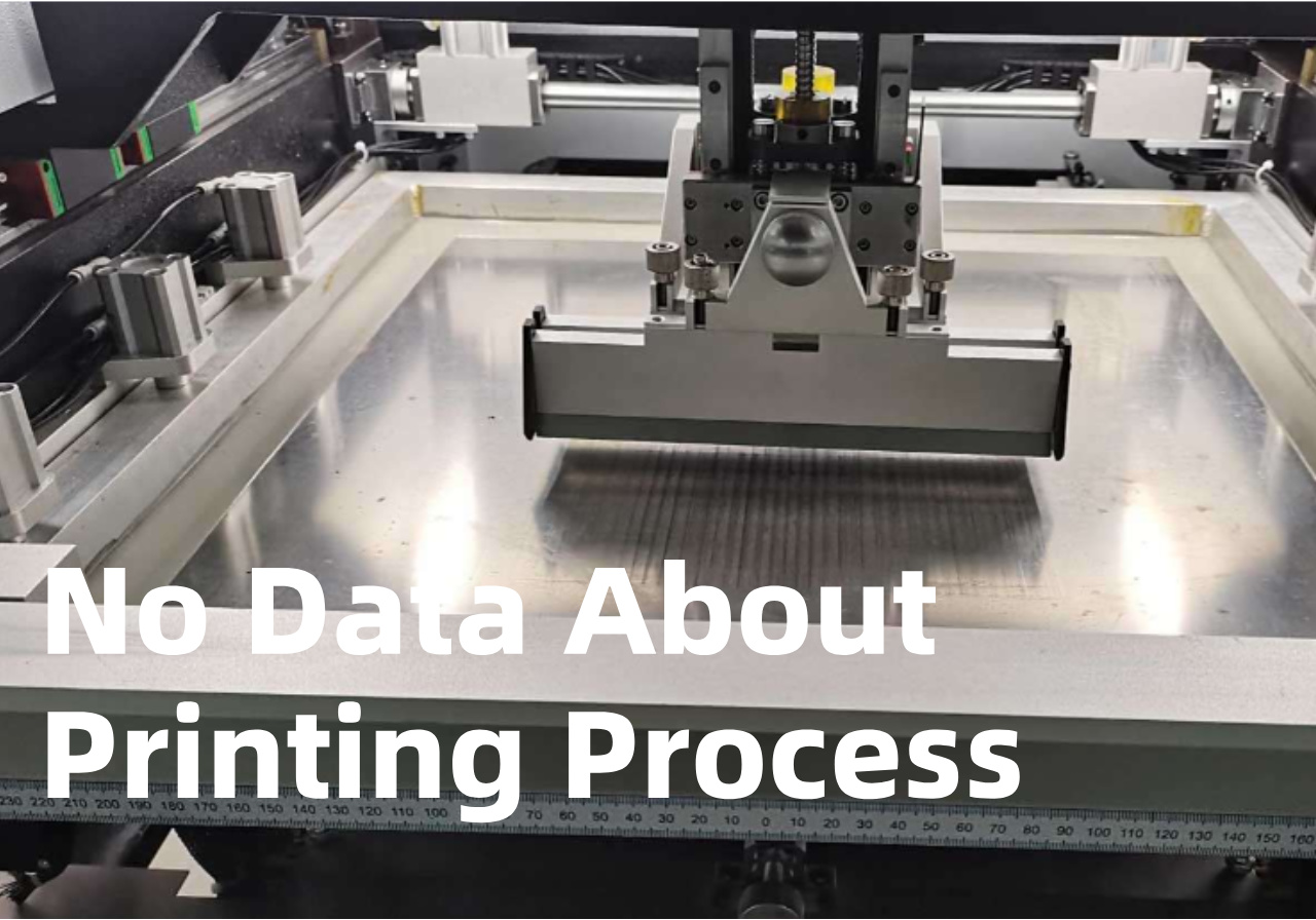
In the morning shift, defects might be only 2%, but the night shift suddenly jumps to 15%. The machine program is exactly the same, the stencil is the same, and the paste is from the same jar. The only difference is the operator. One person might press the squeegee a little harder, another might set separation speed a little faster.
These tiny differences create big volume changes that you cannot see with your eyes. Everyone gets frustrated because no one knows who is “right.” SPI removes the guesswork by measuring every board automatically, so every shift gets the same perfect print, no matter who is running the machine.
You clean the line, install a fresh stencil, run the first few boards, and suddenly AOI is full of red errors. Volume might drop 20-30% on small apertures, or bridges appear where they never existed before. This happens because every new stencil has slightly different thickness, aperture size, or surface finish.
Without measurement, you spend the whole day tweaking settings to get back to yesterday’s quality. SPI scans the very first board after a stencil change and tells you exactly which apertures are low or high. You make one smart adjustment and continue production—no wasted boards, no wasted hours.
Imagine a pilot trying to land a plane while covering all the gauges with tape. That is exactly what happens when you adjust squeegee speed or pressure by feel alone. A small change that feels good might actually make volume worse on half the pads.
Operators end up changing settings back and forth all day, and quality never settles. SPI is your cockpit dashboard: it shows height, volume, and position for every pad in real time. You see the numbers, make one precise change, and the problem disappears. Factories that switch to data-driven printing report stable quality within the first week.
When tiny components like BGA, QFN, and 01005 start failing, the rework station becomes the busiest place in the factory. A single bad board can cost hundreds or even thousands of dollars to fix, and customers start complaining about delays.
Everyone can see the money disappearing, but most people still blame reflow or placement. The truth is that almost all these expensive failures begin with poor solder paste printing. SPI stops them before components are even placed, saving huge amounts of time and money.
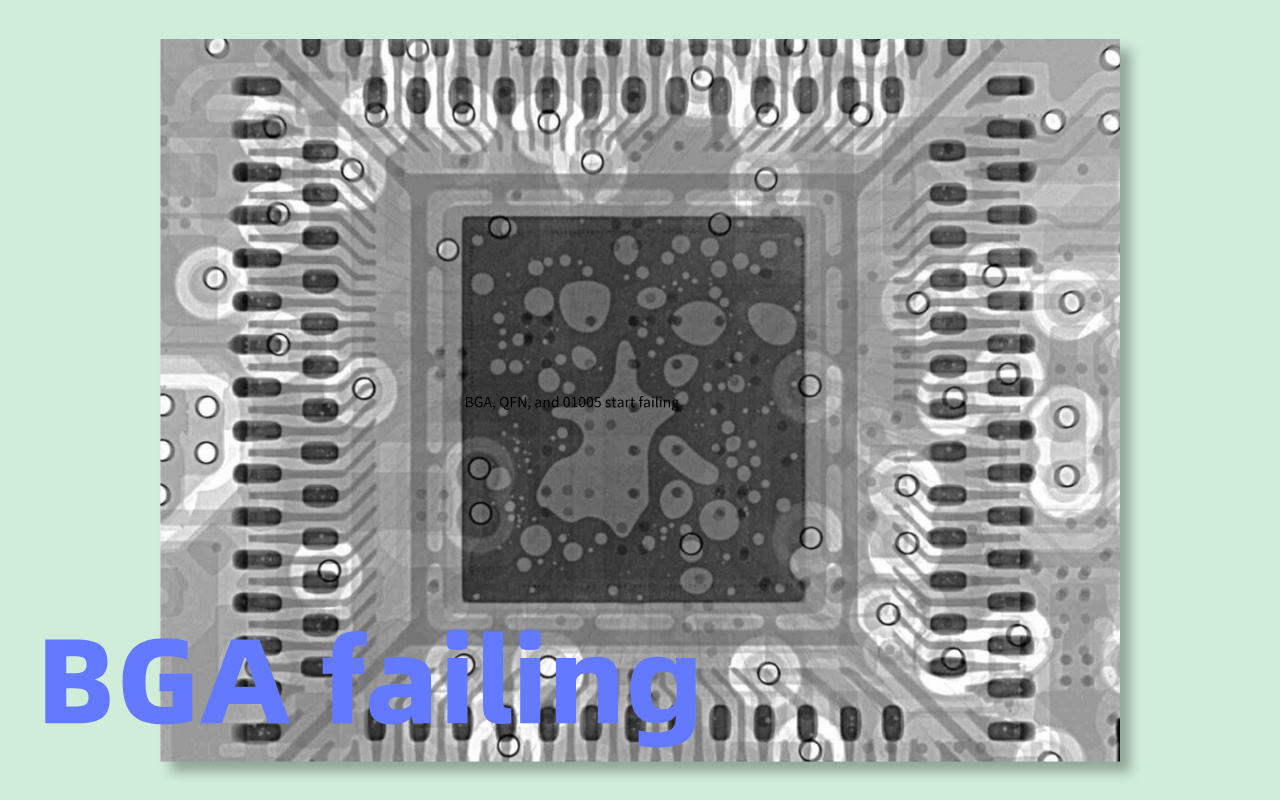
BGA opens mean some balls do not connect at all after reflow. Head-in-pillow looks like the BGA ball is resting on top of the paste instead of melting properly. Shorts happen when too much paste connects two balls. Engineers often say “reflow profile is wrong,” but the real cause is usually uneven paste volume from printing.
If one ball has 30% less paste, it will not wet correctly. Reworking a single BGA can take 30-60 minutes and risks damaging the chip. SPI measures every ball’s paste volume right after printing, so these problems never reach reflow.
QFN devices have pads underneath, so if paste volume is too low on one side, solder will not climb the side wall—this is called poor wetting. 01005 chips are so small that even a tiny volume difference makes one end lift up during reflow, creating tombstoning (the chip stands up like a tombstone).
Both problems are 100% caused by uneven printing. Reworking a tombstoned 01005 is almost impossible without damaging the board. Operators spend hours with hot air guns trying to fix what should have been prevented in seconds. SPI catches volume differences of just a few microns, keeping even the smallest chips perfectly flat.
A 20 μm difference in paste height sounds tiny—it is thinner than a human hair. But during reflow, that small difference grows into big problems: opens, shorts, head-in-pillow, or tombstoning. One bad board can scrap an entire expensive module, like a smartphone camera or automotive sensor.
If you make 500 boards per day, just 5% defect rate means 25 bad boards—and thousands of dollars lost every single day. Multiply that by a month, and the cost easily pays for a brand-new SPI machine. SPI measures height to within 1 μm accuracy, so a 20 μm problem is caught and fixed before the board ever leaves the printer.
Every year your customers ask for smaller, denser, more powerful boards: 0.4 mm pitch BGA, 01005 resistors, Mini LED arrays.
The parts get tiny, but most factories still use the same old printing habits from the 0603 era. That is like trying to win a Formula 1 race with a bicycle. The rules of physics have changed, and if your process has not changed with them, failure is guaranteed.
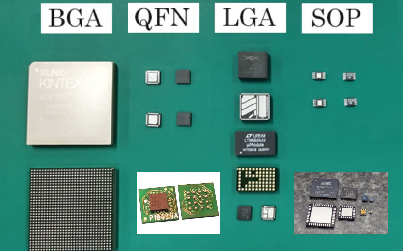
A 0.4 mm BGA has balls only 0.25 mm in diameter and the gap between them is less than 0.15 mm. An 01005 chip is only 0.4 mm × 0.2 mm—smaller than a grain of rice. Mini LED boards can have 5 000–10 000 tiny LEDs on one panel.
For these parts, the allowed solder paste volume window shrinks from ±50 % (acceptable ten years ago) to ±10–15 % today. Even a small puff of air from the air-conditioner can push the paste outside that window if you are not measuring it.
With big 0603 or 0805 parts you could print “a little more” or “a little less” paste and everything still worked. With modern parts there is almost no margin left. A volume difference of just 10 % can turn a perfect print into a dead board after reflow.
The human eye cannot see this difference, and normal 2D cameras in AOI also cannot measure height or volume accurately. You are basically flying blind in a storm.
Waiting for AOI to find printing mistakes is too late. By then the expensive chips are already placed and the board has gone through the oven. Reworking a 0.4 mm BGA or Mini LED panel is extremely difficult and often damages the board permanently.
Many factories learn this the hard way when a new product introduction fails and customers threaten to move orders elsewhere. SPI gives you the data you need before you place a single component, so the new, difficult product launches smoothly on the first try.
Your team has a strong feeling that something is wrong with the printer, but nobody can prove it.
Meetings go on for hours: “Is it the squeegee? The paste? The stencil? The temperature?” Everyone has a different opinion because nobody has real numbers. This is the most dangerous warning sign of all—when suspicion is high but data is zero.
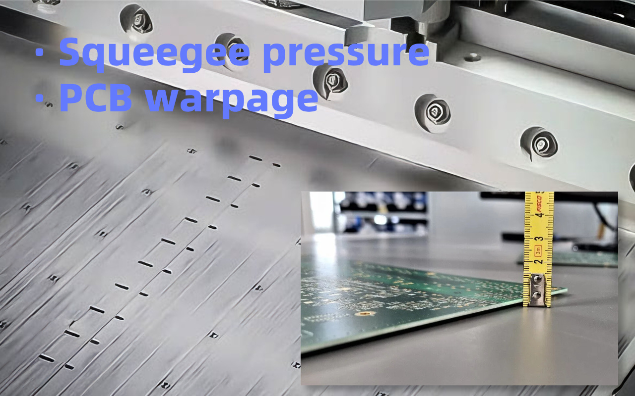
The squeegee blade should push the paste with exactly the same force from left to right. In reality, worn cylinders or dirty rails can make pressure differ by 0.5–2 kg across the stroke.
That small change can reduce paste volume by 20–40 % on one side of the board. You will never feel it by hand, but the boards will show it after reflow.
Modern thin PCB (0.6–0.8 mm) bend easily under their own weight or from heat. A bend of only 100–150 μm is enough to make paste volume vary 30 % between the center and the edge of the panel.
Operators see bridges or insufficient solder but cannot explain why. SPI instantly creates a 3D warpage map and volume map in one scan, so you know exactly where the problem is.
Solder paste is sensitive to room temperature humidity. A 5 °C rise or 10 % humidity drop can make the paste roll differently and change volume by 15–30 %. A new batch of paste from the same supplier can behave completely differently because of tiny changes in metal content or flux.
Without SPI you only discover this after hundreds of bad boards. With SPI you see the change on the very first board of the new batch and adjust in seconds.
If you recognise even two of the five signs above, the message is clear: your printing process is out of control and costing you money every single day. The good news is that the fix is simple and fast.
☐ AOI keeps stopping boards for the same paste issues (volume, bridge, offset)
☐ SMT Printer settings changed almost every shift with no lasting improvement
☐ Rework station is full of fine-pitch BGA / QFN / 01005 failures
☐ Your next product uses 0.4 mm or smaller pitch or Mini LED
☐ You argue about printer problems but have no hard numbers to prove anything
Two or more checks = your factory is already losing thousands of dollars every week.
Most companies wait until a major customer audit, a huge field failure, or a lost contract before they finally install SPI. By then they have already thrown away six to twenty-four months of profit. Smart factories install SPI before the pain becomes unbearable.
The machine usually pays for itself in 6–12 months through lower rework, higher yield above 99 %, and zero customer complaints. The only question left is: do you want to keep paying the “stupid tax” or start saving money today?
No. AOI sees the top surface after component placement; it cannot measure solder paste volume, height, or coplanarity before components are placed. Industry data shows 3D SPI prevents 60–80 % of defects that AOI would otherwise catch too late.
Modern inline 3D SPI systems achieve 30–80 cm²/s inspection speed with full 3D measurement—faster than most high-speed placement machines. Cycle time impact is typically <3 seconds per board.
Typical payback period is 6–12 months via rework/scrap reduction alone. High-mix factories often see ROI in <6 months; automotive/medical/aerospace achieve ROI in 3–9 months due to zero-escape requirements.
Even stable products suffer from stencil wear, paste batch variation, and environmental drift. Factories running only one product for years still report 3–8 % yield improvement after installing SPI.
Calculate your current rework + scrap cost per month on paste-related defects, multiply by 12, then compare to SPI price. The math almost always speaks for itself within one slide.